ZX97 Micro Computer
Revised Dec 1 ,
1997
(c) wilf rigter
The
ZX97 is a discrete logic clone of the ZX81. It is functionally
equivalent
and 100% compatible but has numerous enhancements over
the
original ZX81. The all CMOS design draws only 50mA and can
be
easily powered from a small battery.
The
total memory is increased from 9K to a 192K including 32K of
EPROM
and 160K of battery backed up SRAM. A SHADOW RAM feature
allows
users to enhance or replace the ZX81 operating system with
the
ZX80, FORTH or any other OS software.
The
16 parallel bi-directional I/O lines are connected to an IBM
compatible
printer port (LPT1) and can also be used for high speed
communication
with a PC or for robotics applications.
Aside
from the existing ZX81 screen text and graphics, the ZX97 offers
a
full 128 upper and lowercase text characters and unlimited user defined
graphics
(UDG) And finally, the ZX97 supports both pseudo hires and true
bitmapped
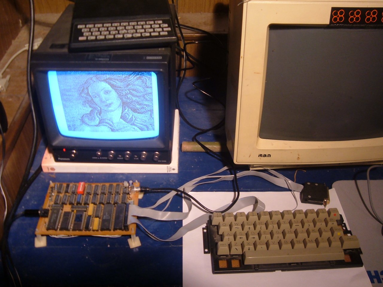
graphics (192x256) programs. Here is a look at the ZX97
Prototype
The
ZX97 circuit is described in functional blocks as shown in FIG 1.
and
circuit details are shown in the schematic FIG 2.
CRYSTAL
TIMEBASE / MEMORY MAPPER CIRCUIT
-----------------------------------------
The
circuit in Fig 2A generates the 6.5MHz video clock, the 3.25MHz
CPU
clock and the 15.75KHz horizontal clock.
The
6.5 MHz crystal clock is divided by 2 with one stage of 74HC74 to
generate
the CPU clock. The 74HC393A dual 4 bit counter together with
the
74HC11 divides the CPU clock further by 207 to generate the 15.75 KHz
horizontal
frequency. The 74HC08 generates 4.6 us wide HSYNC pulses
which
are gated by the VSYNC and NMI latches before routing to the
video/sync
mixer and the CPU NMI input. The counter is also held reset
during
the VSYNC period to maintain synchronization between the software
generated
VSYNC and the hardware generated HSYNC (in the FAST MODE).
MEMORY
MAPPER
A
novel memory decoder using a 74HC251 generates the memory chip select
signals.
ZX97 system memory map is as follows: 0-8K EPROM or SHADOW RAM,
8-40K
system RAM, 40-48K EPROM (extended OS) and 48-64K bank switched
EPROM/RAM
DISK memory. The memory segment 32-40K is used as system RAM or
can
be mapped over the 0-8K area to install and test a modified BASIC
or
other operating system by closing SW1. In that case the 0-8K RAM is
write
protected and the 0-8K EPROM segment is remapped to 32-40K. Note
that
the 74HC251 is enabled with MREQ or RFSH to access the video pattern
data.
The RAMDISK is also enabled by the ROMCS signal but the DISKON signal
disables
the EPROM /OE and enables the RAMDISK CE in the 48-64K area.
ZX97
CPU/SYSTEM MEMORY
----------------------
The
ZX97 uses a CMOS Z80A CPU for reduced power consumption.
Details
of the Z80 can be found in the ZILOG literature.
Fig
2b show the RAM and EPROM chips which are also low power CMOS.
Parts
of the video circuit which address the memory at REFRESH time
includes
the CHR$ latch which generates part of the pattern table
address
from the CHR$ code. The 3 bit LCNTR is incremented with HSYNC
and
generates the pattern table 3 LSB address bits. The CPU I register
generates
the pattern table base address. Additional circuits disable
the
pattern table address circuit when A14 is high for TRUE HIRES programs.
Loading
an odd byte value into the I register enables the expanded pattern
table
offering 128 unique character pattern shapes.
SYSTEM
RAM and EPROM
Both
system RAM and EPROM are 32K byte CMOS devices. The RAM is battery
backed
up and write protected in the 0-8K segment to avoid corrupting the
shadow
RAM data from spurious writes when switched to the 0-8K segment.
The
EPROM will be changed in a future revision to a 128K byte device
providing
64K of EPROM DISK and 64K of paged OPERATING SYSTEM code.
ROW
COUNTER / CHR$ LATCH
The
Sinclair text mode is supported with a pattern table in EPROM at address
1E00-1FFF.
User Defined Graphics (UDG) RAM pattern tables are also supported.
UDGs
are accessed by changing the I register to point to the new pattern
tables
in RAM or EPROM which must be located in 0-16K or 32-48K. One half
of
a 74HC393 dual hex counter is used as a modulo 8 line counter which
increments
every HSYNC pulse and during RFSH time it addresses the 8 lines
of
patterns for each character. The line counter is reset with VSYNC.
The
74HC374 CHR$ latch is loaded with each DFILE character code and during
RFSH
it is used to address the corresponding pattern table entries.
Two
bits of the 374 and a 74HC125 are used to provide tristate outputs for
the
line counter.
ZX97
RAM / EPROM DISK
---------------------
Fig
2c shows the simple circuit
requirements to provide 128K of RAM DISK.
The
RAM DISK is accessed at 48-64K (C000-FFFF) in 8 pages of 16K each using
the
8255 Port PB0-2. PB3 is used with
A14-15 to select 8 pages of RAMDISK
or
one page of EPROM disk. PB4 is used for write protection and a manual
write
protect
switch is also included. A RAMDOS program is included in EPROM which
makes
it easy to save and load program, variable and binary files.
ZX97
VIDEO LOGIC
----------------
In
the Sinclair video system, the CPU is a key element in the display
circuit.
Most other PC's use a separate video controller with video memory
access
multiplexed between the CPU and the video controller.
In
the ZX81/97, the CPU is multitasking between application program
and
display file execution. During video task execution, the Z80 is used
to
sequentially read character codes from the "screen memory" which is
a
segment
of system RAM pointed to by the system variable DFILE.
Then
the CPU, together with the line-counter and CHR$ register, generates the
pointer
to the pattern byte which is loaded into the video shift register
and
clocked out as a video bit stream. During true high resolution graphics
mode,
the CPU does all the work, pointing directly to the bit mapped patterns
in
a 6K hires display file which are sequentially loaded into the video
shift
register. For more detailed information, see the ZX81 Video Tutorial.
THE
NOP LOGIC
An
important element in the video circuit is decoding access to the DFILE.
When
a valid CHR$ code is read from the video display (DFILE) , the NOP LOGIC
(74HC138)
and a 74HC08 AND gate decodes this condition. The NOP LOGIC output
turns
on a 74HC245 buffer to "force" a low level on the CPU data bus
thereby
tricking
the Z80 into executing NOPs during DFILE execution.
VIDEO
SHIFT REGISTER/VIDEO INVERT LOGIC/VIDEO SYNC MIXER
The
NOP LOGIC is used to generate the video shift register load signal
if
a valid CHR$ is read from DFILE. Since this occurs at the end of the
"forced"
NOP, the NOP LOGIC output is saved in the NOP register (74HC74A)
on
the rising edge of RD. The NOP register is clocked into the S/L register
(74HC74B)
on the rising edge of the T1 decoder (74HC08). Feedback to the SET
input
of the NOP register resets the S/L register after a 30 nsec gate delay.
This
generates a 30 ns pulse to load the pattern byte into the video shift
register.
The D7 bit of the CHR$ code is saved in the D7 register (74HC74A)
on
the rising edge of RD and is clocked into the INVERT register (74HC74B) on
the
rising edge of the LOAD PULSE at the same time as the pattern byte is
loaded
into the video shift register.
The
video shift register is loaded with the video pattern data from RAM
or
EPROM, the pixels are clocked out at 6.5 MHz and the pixels are inverted
with
a 74HC86 if the INVERT register bit is set.
The
output from the 74HC86 XOR gate is passed through a 74HC74 video
synchronizer
flip flop eliminating any effects of differential time delays
between
the VIDEO input and the INVERT inputs of the XOR gate.
The
CSYNC signal is connected to the serial input of the shift register to
produce
a black level (back porch) after each sync pulse.
The
video is combined (mixed) with the CSYNC signal to produce a composite
video
signal suitable for connecting to a video monitor or RF modulator.
ZX97
GRAPHICS
New
pattern tables in 32-40K RAM can be used to enhance the normal
Sinclair
text mode. A new "extended" Sinclair text mode has been added
which
provides 128 unique character patterns (ie upper and lower case).
In
the ZX97, the video pattern tables are located in both EPROM and RAM
(unlike
the ZX81) providing user definable character (UDG) sets.
Pattern
data is read during RFSH with the I register and the ROW counter/
CHR$
latch hardware.
Both
true hires software based on WRX16 and HRG algorithms and the
"pseudo"
hires programs like Rock Crush are supported by the ZX97.
True
High Resolution graphics programs (ie WRX16) fetch pattern data
from
system RAM using the I and R registers and the pattern table lookup
hardware
has to be disabled. A high on A13 or
A14 is used to disable
the
ROW counter/CHR$ latch tristate outputs during RFSH.
The
memory map for Sinclair character and pseudo hires patterns is 0-8K.
For
UDG and 128 character text, pattern data must be located in 32-40K.
All
other parts of the memory map are true hires.
Pseudo
Hires is supported without any changes to provide downward
compatibility
with many excellent programs such as Rock Crush.
For
future software development, UDG's and True Hires would appear
more
logical choices, given the new ZX97 hardware features.
ZX97
I/O CIRCUIT
----------------
The
ZX97 I/O circuit in Fig 2e includes the keyboard logic, TAPE IN/OUT
logic,
part of the SYNC/NMI logic which is I/O mapped and the 8255 logic.
To
maintain compatibility with the ZX81 I/O port assignment, the same
incomplete
I/O address decoding is used for I/O address bits 0-3.
A
few 74HC32 OR gates provide the necessary logic to access the NMI and
SYNC
latches. A more conventional I/O decoding circuit is used to
generate
address DF for the 8255 24 bit parallel interface controller.
KEYBOARD
LOGIC
The
ZX97 keyboard interface uses the same A8-15 row scanning as the ZX81
and
the five keyboard data lines are connected to bits D0-4 of a 74LS245
tristate
buffer. The output is enabled with IN FE to read keyboard colunm
data.
Two other bits (D6-7) are used to sense the 50/60 Hz option and the
TAPE
input.
THE
TAPE INPUT/OUTPUT
The
TAPE INPUT is compatible with ZX81 as well as the ZXTAPE system for
PC<>ZX
data transfer using a simple 2 wire cable connected to the PC
Printer
port. Data is saved and loaded with the build in functions.
The
"easy to use" ZXTAPE.EXE program takes care of the PC hardware.
The
TAPE OUT signal (actually the VSYNC) is a TTL level suitable for
line
in of a tape recorder and is also connected to STATUS input of
the
LPT1 connector.
NMI
AND VSYNC LATCHES
Two
SR latches are used to control the flow of NMI pulses to the CPU and
SYNC
pulses to the VIDEO/SYNC MIXER. The NMI latch is set with OUT FE
which
gates the NMI pulses to the CPU and is reset with OUT FD.
The
NMI latch, when off, also enable the set input of the VSYNC latch.
The
action of the SYNC latch is a little more complicated because it
produces
a VSYNC pulse which is XOR'd with the HSYNC pulses to generate
a
negative sync level for as long as the VSYNC latch is set.
The
SYNC latch, which is set with IN FE, also resets the 15.75 KHz counter
to
maintain synchronization between the VSYNC and HSYNC in the FAST mode.
The
XOR gate inverts the inactive HSYNC output and thereby generates the
negative
vertical VSYNC pulse. Any OUT command resets the VSYNC latch,
terminates
the VSYNC pulse and enables normal HSYNC pulses.
8255
PARALLEL I/O PORT
The
8255 is a general purpose parallel I/O port. The 8255 defaults to
3
input ports on reset and to configure ports for output, a control word
must
be written to the control register located at address DF.
Port
A is generally used as a high speed interface to a PC printer port.
Port
B is used for control of the RAM disk and Port C is used for hand
shaking
with the PC printer port. Of course Port A and C can be used for
any
general purpose parallel I/O.
The
8255 is accessed at I/O address DF and the internal registers are
addressed
with A3 and A4. Therefore the control register is at port DF
and
the data registers for ports A to C are addressed at C7, CF and D7.
Note:
Port C output bits can be accessed at two different locations.
Port
C output byte is accessed at D7, but in addition, individual
Port
C bits can be set or reset at address DF with control word values
00
to 0F. Even values 02 to 0E reset bits 0 to 7 respectively and odd
values
01 to 0F set bits 0 to 7.
____
|
6.5|--->-------------------------------------------------------------+
| | _______
_____________ |
|XTAL| A14-->|RAMDISK|
+--------->|/CE A13|<---
PB0 |
|TIME| A15-->|DECODE | | | RAM DISK A14|<----PB1 |
|BASE|
PB3-->|_______|-|-----+--->|CE A15|<----PB2
|
| | |
| |_____________| |
|____| _____
______ | __V__
_____ _____ _____
|
|
CPU| | CPU | |MEMORY|
| | OE | | |
| ROW | |VIDEO| |
|
CLK| | MREQ|-->|DECODE|--+->|
A0-2|->| A0-2|<----| CTR | | S/R
| |
|
/2 | | | |______| | RAM |
|EPROM| |-----| |
CLK|<+
| |
|
ADR|->-+----[2K]--->|A3-8 |->|A3-8 |<----| CHR | |
|
|
3.2|--->|CLK | |----------->|A9-14|->|A9-14| |LATCH|
| SOUT|-+
| |
| DATA|<--|-+--[2K]--->|D0-7 |->|D0-7 |--+->|D0-7
|->|_S/L_| |
|____| | | | |
__ | | | |
| |_____| |
|
|HOR
| | IORQ|_ | +-<-|NOP|
|_____| |_____| _V_______ |
|
|NMI
| +->|NMI | | | |___|<-----------------| D6/7 |-->---+ |
|GEN
| | |_____| | |__________ |NOP LOGIC|
_____ |
|/207|
| _____ | ________ |
_____ _____
|_________|-->|VIDEO|<+
| | +--| NMI | |_| I/O | | |KEYBD| | 8255|
_____ |INVRT|
|15.7|--->|/SYNC|<--|
DECODER| +>|LOGIC| | I/O | |VIDEO|<-|_____|
|
RST|<---|LATCH| |________| |_____|
|_____| |/SYNC|
|____| |
|--> ROW CNTR RESET
| |MIXER|--> COMPOSITE
|
|_____|----------------------------|------->|_____| VIDEO OUT
| |____________
+-->ROW CNTR CLK FIG 1 - ZX97 BLOCK DIAGRAM `----> to PC LPT
VIDEO CLOCK HSYNC/NMI TIME BASE
6.5 MHz 15.7 KHz
__|-|___ ______
|
|-| | |393A R|___________________________________
|
| CPU CLOCK |
R|___| __ |
|-[10M]--| 3.2MHz | Q1|--------------------|11 \ __
|
| __
[2K] _____ |
Q2|--------------------|
>--)32 \__|
+--|00 \_|_____|C Q|_ | | __ +-|__ /
+-)__ /
+--|__ / | | 74C | | Q3|-----------|11 \ |
|
6.5
------| __|D /Q|__ | Q4|--+--------| >-+ |
|
| |__R__| | | CLB|__| +-|__ / |
/6.5
_/|__| |___________| |
Q5| | |
\| 0V | |
Q6| __ | |
3.2M ___________________|__|CLA Q7|--|08
\__| |
| Q8|--|__ / | |
|______| | |
HSYNC
____________/|_________________________| |
\| 74HC04 |
VSYNC
________________________________________________________|
RAMCS
________________________________________________________
ROMCS
__________________________________ |
__ | |
RFSH -----|08 \____ | |
RD -----|__ / |
| |
+5V |
| |
| |
| +5V |
SW1
[10K] | __
_____ | | |
0V____/
___|__|\__ +--)32 \____|0 251| |
[2K] |
SHADOW
| |/ `----)__ / |_|5 Y|_|___| |
RAM
|____________________|4 |
0-8K+ |
|_|1 |
40-64K +5V |
0V
_____________________________|2
| | |
0V
_____________________________|3
| [2K] |
| | 8K-40K | |
M1
_____________________________|6
W|____________|__________|
M1
_____________________________|7 |
A13_____________________________|A |
A14_____________________________|B |
A15_____________________________|C |
__ | |
RFSH
--------|08 \______________|E |
MREQ
--------|__ / |_____|
Figure 2a - ZX97
TIMEBASE/MEMORY MAPPER
NOP______________________________________________________________
______ |
NMI_________________________________________________|NMI |
| NOP
| __
| | |
+----)32 \___|WAIT | |
_____
+----)__ / | Z80 |
__|__
WR
--------------------------|WR | |_______/|___|HALT | |
OE |
______ |
| _____ \|
| | | 245 |
D0'---------------| D0|---|
D0|---| D0|-[1K]-|D0 |--|A0 B0|__
D1'---------------| D1|---|
D1|---| D1|-[1K]-|D1 |--|A1 B1|__|
D2'---------------| D2|---|
D2|---| D2|-[1K]-|D2 |--|A2 B2|__|
D3'---------------| D3|---|
D3|---| D3|-[1K]-|D3 |--|A3 B3|__|
D4'---------------| D4|---|
D4|---| D4|-[1K]-|D4 |--|A4 B4|__|
D5'---------------| D5|---|
D5|---| D5|-[1K]-|D5 |--|A5 B5|__|
TRUE
HIRES DECODE | | |
D6|---| D6|-[1K]-|D6 |--|A6 B7|__|
__
_______|OE | |
D7|---| D7|-[1K]-|D7 |--|A7 B7|__|
A14-)32
\_| __ | | |
| | | | |
|__D__| |
RFS-)__
/ `o|125\_|......|---|A0 A0|---|
A0|-[1K]-|A0 | |_____|
+------|__ / | | | |
| | | IORQ|--> |
|
_____ | 374
| |62256| |27256| | MREQ|--> 0V
|__|Q0 Q1|---|D6 Q6|---|
A1|---| A1|-[1K]-|A1 RD|-->
LCNTR
| Q2|---|D7 Q7|---|
A2|---| A2|-[1K]-|A2 WR|-->
| 393B| | Q0|---| A3|---|
A3|-[1K]-|A3 M1|-->
/VSYNC__|R |
| Q1|---| A4|---|
A4|-[1K]-|A4 RFS|-->
HSYNC__|CLB
| | Q2|---| A5|---| A5|-[1K]-|A5 0|<-- 3.2
|_____| | Q3|---| A6|---|
A6|-[1K]-|A6 A6|___
RD----------------|CP Q4|---|
A7|---| A7|-[1K]-|A7 INT|___|
128 CHR$ | Q5|---| A8|---|
A8|-[1K]-|A8 |
DECODE
__ |______| |
| | | | BRQ|--5V
A8-------|00
\__ __ | VDD|---| VDD|------| VDD|--5V
INVERT---|__
/ `----|125\_ | | |
VSS|------| VSS|--0V
RFS --o|__ / `-| A9|---|
A9|-[1K]-|A9 |
| A10|---|
A10|------|A10 |
RAM BATTERY BACKUP | A11|---| A11|------|A11 |
3V LITHIUM
1N34A | A12|---|
A12|------|A12 |
+5 ----+|-----|<-------+ |
A13|---| A13|------|A13 |
VBB
--------------------| | A14|---|
A14|------|A14 |
0V -----------|<----+--| |
/OE|_ | |
| /RST|_____/RST
1uF | |
| /CE|_| | /CE|____
| |
=== |____|VSS | | |
| | |______|
|+ |_____| | | /OE|__ |______________
ROMCS
5V | |_____| |________________ DISKON
|____________________________RAMCS
Figure 2b - ZX97 CPU/MEMORY
CIRCUIT
_______
+5V
------------| Vdd |
D0'
------------| D0 | 128Kx8 SRAM
D1'
------------| D1 | KM681000LP
D2'
------------| D2 |
D3'
------------| D3 |
D4'
------------| D4 |
D5'
------------| D5 |
D6'
------------| D6 |
D7'
------------| D7 |
A0'
------------| A0 |
A1'
------------| A1 |
A2'
------------| A2 |
A3'
------------| A3 |
A4'
------------| A4 |
A5'
------------| A5 |
A6'
------------| A6 |
A7'
------------| A7 | +5V
A8'
------------| A8 | +5V |
A9'
------------| A9 | | [10K]
A10
------------| 10 | [10K] SW2
__ |
A11
------------| 11 WR|__ |___/ _____
/125|o--+--- PB4 WRITE PROTECT
A12
------------| 12 | \ __|------- WR
A13
------------| 13 |
PB0
------------| 14 |
PB1
------------| 15 | __
PB2
------------| 16 | / |------ A14 RAMDISK
SELECT
ROMCS
__________|/CE CE|---+-----------<
11 |------ A15
|__|/OE | | \ __|------ PB3
VBB-------------|VSS |
|
|_______| |
DISKON______________________|
Figure 2c - ZX97
RAMDISK CIRCUIT
_________
5V ---------------------| MC34164 |-- 0V
5V ----[10K]--+ |_________|
74HC04 ________ LPT1
RST ___________|______________|_______________|\___|RST PA0|--->
D0
| |
|/ | PA1|---> D1
1N4448
KEY MATRIX +| |
RESET | PA2|---> D2
A8
----|<------|-|-|-|-|- 1 uF=== |-
SWITCH | PA3|---> D3
A9
----|<------|-|-|-|-|-
|____| | PA4|---> D4
A10----|<------|-|-|-|-|- | RD ------|RD
PA5|---> D5
A11----|<------|-|-|-|-|- 0V WR ------|WR
PA6|---> D6
A12----|<------|-|-|-|-|- LPT1 |
PA7|---> D7
A13----|<------|-|-|-|-|- SEL <---|PC4
PC0|---> STB
A14----|<------|-|-|-|-|- PE <---|PC5 PC1|--->
ALF
A15----|<------|-|-|-|-|- ACK <---|PC6
PC2|---> INIT
KEY PORT | | | | | BUSY <---|PC7 PC3|---> SEL
_____
| | | | |
| |
D0
____|A0 B0|_| | | | |
D0------|D0 |
D1
____|A1 B1|___| | | | D1------|D1 8255 |
D2
____|A2 B2|_____| | | +5V D2------|D2 PB0|--->PB0
D3
____|A3 B3|_______| | | D3------|D3 PB1|--->PB1
D4
____|A4 B4|_________| [10K]
D4------|D4 PB2|--->PB2
D5
____|A5 B5|___ 0V | 50Hz D5------|D5
PB3|--->PB3
D6
____|A6 B6|_____________|__/ __0V
D6------|D6 PB4|--->PB4
D7
____|A7 B7|________________ TAPE IN
D7------|D7 PB5|--->NC
___|OE
D|___ 0V | | PB6|--->NC
|
| 245 | [100K] A3------|A PB7|--->NC
|
|_____| | A4------|B CE|____
|__________________ 0V |________| |
| I/O ADDRESS _____ DF |
| DECODER A5-----|A 3|____|
| A6-----|B 138|
| A7-----|C |--FUT I/O
__ | M1-----|E |--FUT I/O
A0
--)32 \__ __ | VSYNC
IORQ---|/E |--FUT I/O
RD
--)__ / `--)32 \__| __
LATCH 0V-----|/E |
+--)__ / `-----)32 \__ __ |_____|
| IN FE +-)__ /
`--|00 \____________________/VSYNC
| (VSYNC ON) |
+-|__ / | |
__________ HSYNC
IORQ
-------+ | |________|__ | |
__
| |
________| | | +-))86 \___ CSYNC
| __ | |
__ | +-|-))__ /
+--)32 \__ |
+-|00 \_____|___|__________ VSYNC
WR
------------)__ / +---|-----------|__
/ | __
OUT NN |
|__________________ +--)32 \___ NMI
(HSYNC ON) | __
NMI LATCH| +------)__ / ____
+----)32 \__ __
| | __ | 393|
A0
-------------------|----)__ / `---|00
\__| | --|00 \__ | Q0|-
OUT FE | +-|__
/ |
| --|__ / |
Q1|-
(NMI ON) |
|________|__| --|R
Q2|-
| ________| |
__ --|C Q3|-
OUT FD | __ |
__ | --|00 \__
|____|
(NMI OFF) +----)32 \__ +-|00 \_____| --|__ /
A1
------------------------)__ / `---|__
/ NMI-ON SPARE GATES
Figure 2d- ZX97 I/O
CIRCUIT
1N4448 +5V
CSYNC
--------------------------|<--------------+--[1K]--|
/6.5M
_____________________
| |
______ |
VIDEO | |
HSYNC-|SIN | |
SYNCHRONIZER | |
6.5M--|CLK | |
_____ | |
D0`---|D0
165| VIDEO __ |_____|CP Q|- | | C
D1`---|D1 S0|------))86 \___ | 74C | | |/
D2`---|D2 |
+--))__ / |___|D /Q|--[1K]--+------| 2N3904
D3`---|D3
|
| VIDEO |_____| B |\
D4`---|D4 |
| INVERTER | E
D5`---|D5 |
| __ VIDEO
|2|
D6`---|D6 |
|__/ 86((-----+-[10K]--5V
LEVEL P1 |0|<---@ VIDEO
D7`---|D7 | \ __((--+ | NORM/INV
ADJUST |0| |
OUTPUT
__|S/L
| | |__/ ____0V 0V__|_____|
|
|______|
|__________________________
|_____________________________________________|__ `--------> INVERT
__ T1 DECODER INVERT REGISTER |
|
MREQ--|08
\_____ D7 REGISTER _____
| |
3.2
--|__ /
`-------------------+--|C
Q|_ | |
_____ |
| 74B | | |
RD________________________|C Q|___|__|D
/Q|___| |
| | 74A |
| |_S_R_| |
_______|__|D /Q|_
| |_| |
| | |_R_S_| |
+5V |
| | |_| | |
NOP LOGIC
| | +5V | |
_____
| | +5V
| +5V |
HALT--|E |
| | __|__
| __|__ |
M1----|/E |
| |__|C R Q| |__|C S Q|_ |
D6'---|/E |
| __ | 74A | | 74B | |
D7'---|A O7|--+-|08 \____|D /Q|______|D /Q|______|
A14---|B O6|----|__ / | |__S__| | |__R__| LOAD |
A15---|C
138| | | NOP
|_____| PULSE |
|_____| | |
REGISTER CCT |
NOP_____________________| |______________________|
Figure 2e - ZX97 VIDEO CIRCUIT