EZ80 Micro Computer
27 dec 1997 revision
(c) Wilf Rigter
Introduction
------------
The
EZ80 (pronounced "eazy 80") is an all CMOS Z80 controller with some
novel
features. The simple design, powerful debugging features and low
power
(>10 ma) consumption make it suitable for battery powered robotics
hand-held
and/or educational applications. The EZ80 consists of a CMOS
Z80,
32K of battery backed up CMOS RAM, a CMOS 8255 with 24 I/O lines,
and
four simple 74HC type glue chips. "No EPROM!", you say? But how...?
The
big feature of the EZ80 is the "blank slate" memory and the unique
on-board
programming hardware which does not need a monitor program in
EPROM. This is similar to some single chip micro
controller chips which
have
on chip EEPROM programming capability. The EZ80 programming is
performed
using a standard IBM PC printer port (LPT) connection and PC
programming
(EZ80.COM) software. The EZ80 single stepper circuit is
combined
with op codes and data from the printer port to generate random
access
addressing to program the on board non-volatile memory and
perform
a range of debugging functions. The EZ80.COM program so far
provides
the following functions:
1.
FILE 8. BREAKPOINT
2.
LOAD 9. RUN
3.
SAVE 10.RESET
4.
VERIFY 11.SETUP
5.
LIST 12.SHELL
6.
STEP 13.USER
7.
TRACE 14.EXIT
The
programming functions operate on single bytes or blocks of up
to
32K bytes. Program code is normally stored in the 0-16K block which
is
non-volatile and write protected. The read/write data is stored in
the
16K-32K block. A 8255 is a 24 bit parallel interface with four
registers
corresponding to 3 general purpose 8 bit TTL compatible I/O
ports
and a control register. While all 24 I/O pins are available for
small
standalone applications, the EZ80 I/O design is focused on
emulating
an IBM PC printer port to take advantage of the many LPT
peripheral
projects designed for the PC. Conversely any EZ80 I/O
expansion
project should be compatible with the PC LPT port as well!
Port
A is a true bi-directional data port which can be connected to any-
thing
from a printer to a PC printer port. In fact, during programming,
it
is connected to the PC LPT data lines and is used for writing opcodes
and
data to the CPU and data to the memory. Port B has added hardware to
interface
with a 64 contact keyboard matrix. Port C is in fact two 4 bit
I/O
ports used to emulate LPT type control and status lines. A special 4
bit
port is required to multiplex EZ80 data bytes into high and low data
nibbles
suitable for interfacing with the PC LPT status lines. This is
done
with a 74HC257 only used during programming. The 5th status line is
connected
to the Z80 HALT line to monitor and trap Break Points during
debugging.
During programming, a 74HC1389 decoder and 74HC02 NOR gate
generate
the necessary internal control signals from the four PC LPT
control
lines.
With
it's build-in DB25 connector matching the PC LPT pin-out, the EZ80
can
be connected using standard PC connecting cables to a printer or PC,
or
digital and analog I/O expansion units which we will design in future
articles.
As a bonus, these I/O expansion units can also be used with
any
IBM PC.
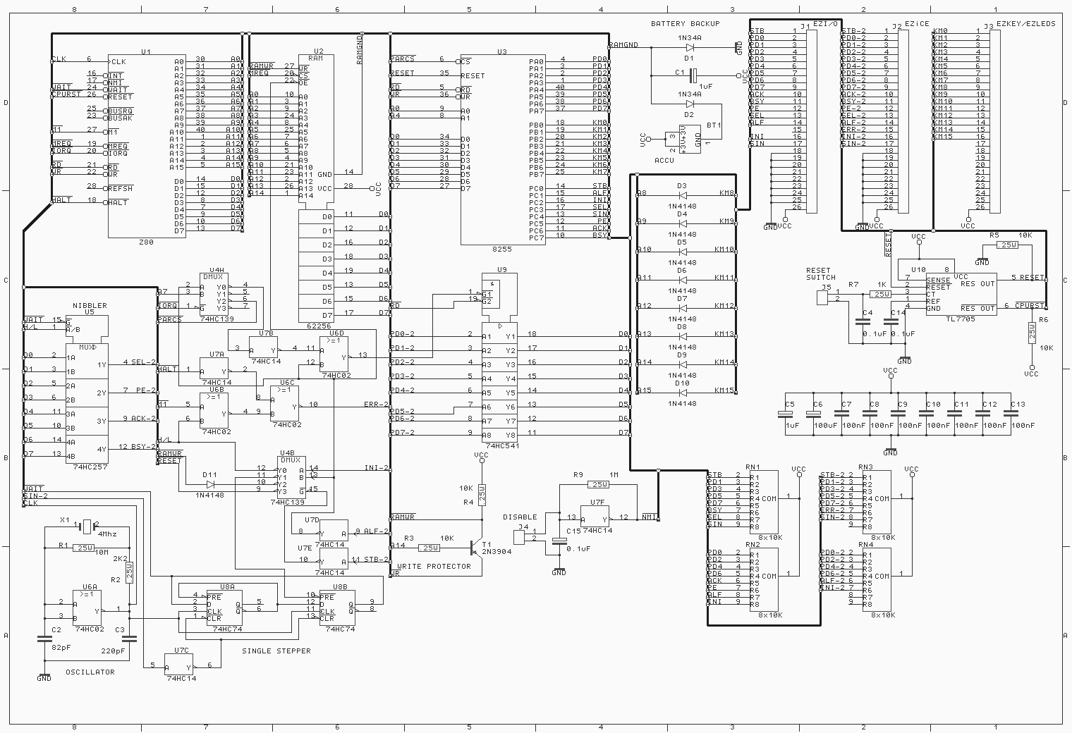
Circuit
Overview
----------------
The
EZ80 circuit details are shown in the schematic fig 1. The circuit
consists
of a Z80 connected straight to a 32K SRAM and 8255 PPI chip.
The
CPU clock is provided by a textbook CMOS gate 4 MHz crystal
oscillator.
Chip count and circuit simplicity are key factors in the
EZ80
design so no additional memory or I/O decoding is provided. The
single
stepper uses a dual 74HC74 D flip flop instead of the more common
monostable
to produce a two clock cycle positive "run" pulse to the Z80
WAIT
line to step to the next bus cycle. The
CPU uses bus cycles to
access
memory or I/O devices and this can be a M1 opcode fetch or any
other
read or write cycle. The WAIT line is usually used to lengthen
CPU
bus cycles to synchronize the CPU bus to devices with slow access
time.
In the case of the single stepper, the CPU is held in the WAIT
state
and is advanced one bus cycle at a time by "tugging" the WAIT
line
with a "run" pulse. The RUN command activates the 74HC74 preset
input
to force the WAIT line positive and to allow the CPU to run at
full
speed. The 8255 PPI defaults on power up to all input ports and
this
is used to advantage in the programming circuit to connect the PC
LPT
data lines to the CPU bus. A 74HC138 decoder and 74HC02 NOR gate are
used
with the PC LPT control lines to override the Z80 IORQ, A0,A7,RD
and
WR control signals. When these signals are applied in the correct
sequence,
the PC LPT port can exercise a kind of direct memory access
(DMA)
to the EZ80 RAM and Z80 data bus. A 74HC14 Schmitt trigger is used
as
inverters and to condition some of the PC LPT control lines. The
74HC257
is used to read the RAM data bytes in two nibbles to the four
PC LPT
status lines. The RESET circuit uses a push button or a decoded
reset
command to reset the Z80 and 8255 chips. The MC32164, a TO92
voltage
monitor, also resets the system whenever the Vcc drops below
+4.75
Volts. This prevents undefined Z80 operations during power cycling
which
could corrupt memory or send spurious signals to the I/O pins.
The
RAM is partially write protected with Q1 which gates the Z80 WR line
whenever
the A14 line is low. This provides 16K bytes of write protected
memory
from 0K-16K and 16K of read/write memory from 16K-32K.
What
makes it tick?
-------------------
The
4MHz CPU clock is generated with a text book low power CMOS Pierce
oscillator
using one section of the 74HC02 NOR gate as an inverter with
the
crystal in the feedback path.
Z80
INSIDE
----------
The
EZ80 uses a CMOS Z80A CPU for reduced power consumption. Details
of
the CPU functions can be found in the ZILOG literature. With a minor
modification
to ZX81 ROM code is compatible with the EZ80 hardware and
control
programs can be written in ZX81 BASIC. Without the video, the
INT
and NMI lines are now available on the board for user applications.
Future
projects will customize the ZX81 ROM for use with the EZ80 I/O
and
add such hardware as a DFILE compatible LCD interface.
Lest
we forget
--------------
The
62256 RAM chip, which is also low power CMOS, uses a 3V lithium cell
for
non-volatile program storage. Note the novel use of a common Vdd
line
and the negative battery connection to the RAM Vss line. This
ensures
that the RAM CE and WR lines are disabled by automatically
switching
to Vdd during power-down. In addition, the MC34164 supervisory
circuit
of Q1 pulls the reset line low when Vdd falls below 4.75V
With
the simple one chip memory, no address decoding is required for
the
EZ80. However the WRITE PROTECTOR circuit divides the memory map as
follows:
16K of program memory from 0K-16K is write protected during
normal
program execution and the 16K-32K block is always accessible as
read/write
RAM. All memory is read/write accessible in the programming
mode.
Boot
Strap?
----------
The
EZ80 uses a hardware "boot strap" circuit to program the
"blank"
memory
from power up. This is the same procedure used in the earliest
days
of computers when the "boot strap" program was entered through
the
front panel switches. That toggling procedure was tedious and
only
a short program was loaded through the front panel which was just
enough
to start the paper tape reader to load in the next layer of
operating
system software. The way in which a PC initializes it's BIOS
and
DOS in successively more complex layers follows a similar sequence
but
has evolved so that by now the operator's front panel actions have
been
reduced to, at most, using in the proverbial three finger salute.
In
fact a bank of 12 switches and some LEDs could still be used to
program
the EZ80 but instead we have finally found a useful application
for
the IBM PC, as a high priced front panel for the EZ80.
Printer
Port Rules, OK!
-----------------------
The
EZ80 circuit in Fig 1 shows the connection from the PC printer port
via
the DB25 connector to the 8255 chip, a 74HC257 chip, a 74HC02 NOR
gate,
a 74HC74 dual D flip flop and a 74HC138 decoder chip.
The
74HC138 is used to decode the PC printer port control lines during
programming
to control and override various internal EZ80 signals. The
74HC138
control functions and codes are shown in fig 7 for the relevant
PC
printer port control line states. These functions codes are used to
reset,
single step and run the Z80 and to control the RAM chip RD and
WR
lines. The 8255 port A is connected to the PC printer port data lines
which
are used to control the EZ80 CPU data bus. The 74HC257 is used to
read
the memory data in two nibbles to the PC printer port status lines.
In
the RUN mode, the EZ80 printer port emulates a PC LPT port and can
be
use with various external devices or can directly control 16 external
TTL
I/O lines.
One
Small Step for Man
----------------------
The
novel 74HC74 SINGLE STEPPER circuit controls the Z80 WAIT line to
single
step the Z80 one bus cycle at a time or with the 8255 can force
external
OPCODES (ie NOP) on the Z80 data bus during each instruction
cycle
while the RAM OE line is disabled. The WAIT line is also used to
enable
the NIBBLER circuit allowing the data bus to read on the LPT
STATUS
lines one nibble at a time. I really like this simple Z80
single
stepper circuit which is destined to become a classic. It adapts
itself
to any CPU clock frequency unlike the usual monostable pulse
generator
designs. The single stepper timing states are shown in fig 3.
One
Giant Leap for Mankind
--------------------------
In
the PROGRAM mode, the 8255 is used to place externally generated
opcodes
and data onto the CPU data bus. No initialization is necessary
since
the I/O ports are in the input mode on power up. With the PC LPT
port
data lines on Port A and with control of the RAM OE normal memory
access
is disabled, and the PC can force the 8255 Port A data on the
CPU
bus . This is accomplished with 3 NOR gates which enables the 8255
chip
select and forces port A input data to be read on the CPU data bus.
This
is such a powerful feature that I have only uncovered the tip of
the
iceberg of possibilities. For example, the PC software presently
writes
NOPs to Port A to increment the Z80 program counter (and address
lines)
to desired starting address but it is just as easy and a lot
faster
to write a 3 byte jump instruction to load the PC counter.
NOPs
are still used to STEP through and LIST a block of the memory
contents.
Ideally, the data read by LIST is automatically disassembled
to
mnemonics. (This one is on my wish list
:) During TRACE, the single
stepper
simply advances the Z80 to the next bus cycle without forcing
Port
A on the CPU bus. While TRACEing each bus cycle of the program,
the
contents of the Z80 registers can be examined with a couple of
POP
and PUSH instructions. As you can see this is pretty powerful
stuff
for such a simple circuit! While single
stepping through a
program,
the PC has to write a sequence of instructions which cause
to
Z80 to describe it's present state and then restore everything back
before
executing the next instruction. Any
volunteers?
The
RUN command simply releases the WAIT line and allows the CPU to
execute
the code in real time from a given starting address. This is
useful
to check out subroutines, etc. In order to return control to the
PC
after executing the subroutine or any other code segment we want to
be
able to insert a break point at the point where the PC takes over.
This
can be done by inserting a HALT in the code eg. replacing the RET
instruction
at the end of the subroutine. The Z80 HALT line is connected
to the
fifth PC LPT status line (ERR) and when the HALT instruction is
executed,
the CPU pulls the HALT line low and stops. The PC monitors the
HALT
line and when active, dumps the Z80 registers including the Program
Counter
(PC) and compares the PC to a list of break point addresses and
then
restores the missing instruction.
Row
and Columns
----------------
Like
the ZX81, the EZ80 has a keyboard interface to connect to a 40
contact
keyboard matrix. It uses the A8-15 lines to scan 8 rows and 5
column
data lines are connected to bits D0-4 of Port B at I/O address
FE.
Sound familiar? In order to use the address lines for scanning the
keyboard
rows we can use the Z80 IN A,(C) opcode to read 8 X 5 bits of
column
data on Port A by rotating a low bit through the B register. This
opcode
uses the C register to address the I/O port on the A0-A7 lines
while
the B register appears simultaneously on the A8-A15 lines. The
other
three bits (D5-7) can be used to expand the matrix to 64 keys or
uses
for a tape input, synchronous serial interface or for a bit banger
UART
application. The I/O address of this port is identical to and
compatible
with the ZX81 ULA keyboard port.
Yippie
I/O
----------
The
8255 is a general purpose parallel I/O port. The 8255 defaults to
3
input ports on reset and to configure ports for output, a control word
must
be written to the control register. Port A is generally used as a
byte
wide bi-directional PC compatible printer port Port B is generally
used
as a forty contact keyboard interface. Port C is used for 4 control
and
4 status lines for the PC printer port. Port A, B and C can also be
used
for any general purpose parallel I/O. In a future article,
applications
will be presented which will explore all the features of
this
excellent chip. The 8255 uses the A0 and A1, to address internal
registers.
In the EZ80, the inverted A0 and A4 lines are connected for
ZX81
compatibility and easy to remember hex address codes 00,01,10,11.
The
8255 data registers for ports A, B and C are addressed at 11, 10 and
01
and the control register is located at address 00. These addresses
are
also compatible with the ZX81 at FF, FE, 7F and 7E respectively.
Note:
Port C output bits can be accessed at two different locations.
Port
C is accessed at address 01, but in addition, individual Port C
bits
can be set or reset by writing data values 00 to 0F to the control
register
at address 00. Use even data, 02 to 0E, to reset bits 0 to 7
respectively
and odd data 01 to 0F set bits 0 to 7.
Who
Controls the Controller?
----------------------------
Fig
6 shows how PC LPT control lines are used to control access to the
EZ80
internal bus. The prog/run switch S1, enables the 74HC138 and the
appropriate
LPT control codes can be used to read, write, etc. Fig 7
shows
the state of the LPT control lines as well as the internal control
signals
and the control code which is written to the PC LPT control
register.
This control code value is not straight forward. The value is
made
up from binary weighted values (shown in brackets in fig 6) but
some
bits are inverted with respect to the control line. In other words
writing
a 0 to some control register bits will result in a 1 state of
the
corresponding control line. The STB (1), ALF (2), and SEL (8) bits
are
all inverted but the INI (4) line is true. In fig 7, a plus or minus
indicates
a true or inverted bit. No wonder the odd relationship between
the
control code and the state of the control lines. Note that WR pulses
have
to be generated by writing three control codes in sequence.
Similarly,
writing OPCODES and TRACING bus cycles require a sequence of
control
codes. I have shown one possible sequence but other sequences
which
combine stepping and reading the data bus are also possible. The
thing
to remember is that DATA must be stable at certain times and the
INI
line must be held high while changing the STB and ALF lines to avoid
glitching
of the decoder outputs. This is important because of the slow
rise
and fall times of the LPT port signals. Note the SEL line, which
activates
the single stepper, is conditioned with a Schmitt trigger to
avoid
double stepping.
Wrap
Up
-------
What
can I say about the EZ80 that I haven't already said twice? I was
pleasantly
surprised to discover a number of new ideas/features just
writing
the article. That's always a good sign that there are more ideas
still
to be discovered. This project also
resonates with my contention
that
many interesting things happen at the simple end of the complexity
spectrum.
This is the nurture phase of the EZ80 project where I look for
some
support. The simple hardware, elegant design and interesting
attributes
make the EZ80 "easy" to use for a variety of applications.
Let's
have those ideas, comments, corrections and let's have some fun!
I
suggest using http://www.ts1000.us/boards.htm
for zx81 related discussion
but
feel free to contact me at: wrigter@dccnet.com
Finally
if the ASCII circuit gives you problems, here is a graphic schematic,
many
thanks to Rodney Knaap ez80_files\EZ80
Schematic.gif
enjoy
wilf
-------------------------------------------------------------------------
KEY MATRIX 1N4448
0V 5V 5V
-|-|-|-|-|-|-|-|------------>|-----A8
RESET |
| | -|-|-|-|-|-|-|-|------------>|-----A9
-| [10K]
___|___
-|-|-|-|-|-|-|-|------------>|-----A10
|_______|____|MC34164|
-|-|-|-|-|-|-|-|------------>|-----A11
| +|
|_______|
-|-|-|-|-|-|-|-|------------>|-----A12
[100K]
1uF=== | -|-|-|-|-|-|-|-|------------>|-----A13
| | |
-|-|-|-|-|-|-|-|------------>|-----A14
| 0V
0V
-|-|-|-|-|-|-|-|------------>|-----A15
| | | | | | | | | +5V
|____ __________ | | | | | | | |
___|___
| | | | | | | | | | |
| Vdd |
RESET _____|__|\__|___|\___ | | | | | | | | |_________|PB0
|
|/ |/ | | | | | | | | |___________|PB1 |
| | | | | | |
|_____________|PB2 |
| | | | | | |_______________|PB3
|
5V 5V | | | | | |_________________|PB4 |
| | | | | | |___________________|PB5 |
__|__ ___|___ | | | |_____________________|PB6 |
| Vdd | |
Vdd | | |
|_______________________|PB7 |
| |
| /RST|_|
|_________________________|RST |
| D0|________|D0 D0|_____________________________|D0 |
| D1|________|D1 D1|_____________________________|D1 |
| D2|________|D2 D2|_____________________________|D2 |
| D3|________|D3 D3|_____________________________|D3 |
| D4|________|D4 D4|_____________________________|D4 |
| D5|________|D5 D5|_____________________________|D5 |
| D6|________|D6 D6|_____________________________|D6 |
| D7|________|D7 D7|_____________________________|D7 |
|62256| |
Z80 | | 8255 |
| CE|--------|MREQ |
| |
| A0|--------|A0 A0|--------------------|02 \____|A | LPT
| A1|--------|A1 |
+--|__ / | PA0|-- PD0
| A2|--------|A2 |
| __ | PA1|-- PD1
| A3|--------|A3 |
|--|02 \____|B PA2|-- PD2
| A4|--------|A4 A4|---------------- | -|__ /
| PA3|-- PD3
| A5|--------|A5 |
| __ | PA4|-- PD4
| A6|--------|A6 IORQ|____|\ _______ |--|02 \____|CS PA5|-- PD5
| A7|--------|A7 | |/ `- | -|__ / | PA6|-- PD6
| A8|--------|A8 HALT ____|\ _________ |
_ | PA7|-- PD7
| A9|--------|A9 | |/ |
| | PC0|-- STB
| A10|--------|A10 BRQ|--* J1
| | | PC1|-- ALF
| A11|--------|A11 INT|--* J2
| | | PC2|-- INI
| A12|--------|A12 NMI|--* J3
| | | PC3|-- SIN
| A13|--------|A13 WR|_____________ | |
| PC4|-- SEL
| A14|--------|A14 A14|_________ |
| | | PC5|-- PE
| OE|_____
| WAIT|_____ |
| | | | PC6|-- ACK
| WR|__
| | CLK|_ | |
| | | | PC7|-- BSY
_|VSS |
| | | | | |
| | | | 0V__|VSS
|
| |_____| | |
|_______| | | |
| | | |______|
| | |___________ | _ | _ | _ | __| |__________________ ERR
| | |
| | | |_________
| | |
| | |_________ | NIBBLER
| | |
| | | | _____
|
|_______ | |
| 5V | | D0 _|
|__ SELIN
| 1N34A
| | | | |
| | D1 _| |__ PE
|-->|-------- 0V
| | | | [10K] [10K] |
D2 _| |__ ACK
| 1uF +
| | | | |
___ | | D3 _| |__ BSY
|--)|-------- 5V
|__ | _ | _ | __|__|c | |
| D4 _| |
| 1N34A
| | | | |
b|__| | D5 _|
A/B|______
+-->|--[3V]+- 5V
| | | | __|e
| | D6 _|
S|___ |
3V BATTERY
| | | | |
|___| | D7 _|
| | |
BACKUP |
| | | | 2N3904
| | 257 | | |
| | | | |_____________| |_____| | |
| | | | WRITE PROTECTOR | |
OSCILLATOR |
| | | | |
__|-|___ |
| | | SINGLE STEPPER | |
| |-|
| | |
| |__________________________________| |
| 4Mz
| | |
| | ______________
| |
|-[10M]--| |
| | | | _____
| ___ | _ |
| __ [2K]
| | | | |
__|__ | |
__|__ | |
|
+--|02 \_|_____
| _ | __|__ | __|__|C S Q| | |_|C S Q|_|
| |
+--|__ / | |
| | | 74
| | | 74 | |
|
| |
| | |______|D
/Q|__|____|D /Q|_ |
|
== ===
| | |__R__|
|__R__| | |
| |
| _| |_____________| | |
0V 0V
| |
____________________________ | ______|
|
| | | ___________ | ____________|
| | | | CONTROL |
| | | | DECODER
|___/|___ SEL (8)
| | | |
\|
| |-- | --[1OK]------- | ---------+
| | | | _____
|
| | | |_|0
A|__|_____/|___ STB (1)
| | |---[10K]----------|1 B|_______ \|
| | | __ __|2 C|___
0V |_____ ALF (2)
| | | 5V |
_|3 /E|_____________ INI (4)
| | | | | | |
/E|___ 0V
| | | [10K] | | | E|__
| | | __| | | |_____|
| S1
| | +->|--'__|__ | _ |
_________|____/ ___0V
| +---->|---' | |
+------------->|---+
+---|<--------------> RESET
Figure 1 - The EZ80 Complete Circuit
_______________________________
| __________________________ | ___ CLOCK
| | _____ | _____ | ___ /RUN
| | __|__ | |
__|__ |
| |__|C S Q| |
|__|C S Q|___|____ /WAIT
| | 74 | |
| 74 |
|______|D /Q|__|_____|D /Q|__
|__R__| |__R__|
|______________|_____/|_____ SEL (8)
\|
Figure 2 - The Single Stepper
_ _ _
_ _ _ _ _
_ _ _
CLOCK _| |_| > | |_| |_| |_| |_| |_| |_| |_|
|_| |_| |_
__ ___
SEL __|
> |_____________________________________
_____ ________________________
/RUN > |________________
________
________________
/WAIT _____ > ____| |__________|
Figure 3 - Single Stepper Timming
__|-|___ +5V
| |-|
| CPU /WR = 0 |
| 4Mz
| A14 = 1 |
|-[10M]--|
----------- [10K]
| __
[2k] _ _ RAM /WR = 0 |___ RAM /WR
+--|02
\_|__| |_| |_ |/c
+--|__ /
| A14 ---{10K]--b|
| | |\e
== 82p === 220p |___ CPU /WR
| |
0V 0V
Figure 4 -
Oscillator Figure 5 - Write
Protector
/OE -------------+
_____
|___/|____ STB (1)
A/B ----|0 A|__|
\|
/WR ----|1 B|____________ ALF
(2)
/RST ----|2 C|____________ 0V
/RUN ----|3 /E|____________ INI
(4)
| /E|____________ 0V
| E|__ ____/ __ 0V
| 138 | | PROG/RUN
|_____| |
`--[10K]-- 5V
Figure 6 - Control Decoder
CONTROL CONTROL
<--LPT CONTROL--> LPT <---EZ80
CONTROL SIGNALS--->
FUNCTION CODE
-STB -ALF +INI -SEL DATA WAIT OE A/B
WR RST RUN
READ RAM LOW
14 1 0 1 0
X 0 0 1 1
1 1
READ RAM HIGH
10 1 0 0 0
X 0 0 0 1
1 1
WRITE MEMORY(1) 15
0 0 1 0 X
0 1 1 1 1
1
WRITE MEMORY(2) 11
0 0 0 0 STABLE 0
1 1 0 1 1
WRITE MEMORY(3) 15
0 0 1 0 STABLE 0
1 1 1 1 1
WRITE OPCODE(1) 15
0 0 1 0
X 0 1 1 1
1 1
WRITE OPCODE(2) 07
0 0 1 1 STABLE 0
1 1 1 1 1
WRITE OPCODE(3) 15
0 0 1 0 STABLE 1*
1 1 1 1 1
TRACE OPCODE(1) 14
1 0 1 0 X
0 0 1 1 1
1
TRACE OPCODE(2) 06
1 0 1 1 X
0 0 1 1 1
1
TRACE OPCODE(3) 14
1 0 1 0 X
1* 0 1 1 1
1
RESET
12 0 1 0 0
X X 1 1 1
0 1
RUN
08 1 1 0 0
X 1 0 1 1
1 0
NO FUNCTION
15 0 0 1 0
X 0 1 1 1
1 1
1* = positive pulse for 2 clk periods
Figure 7 - Control Function Codes