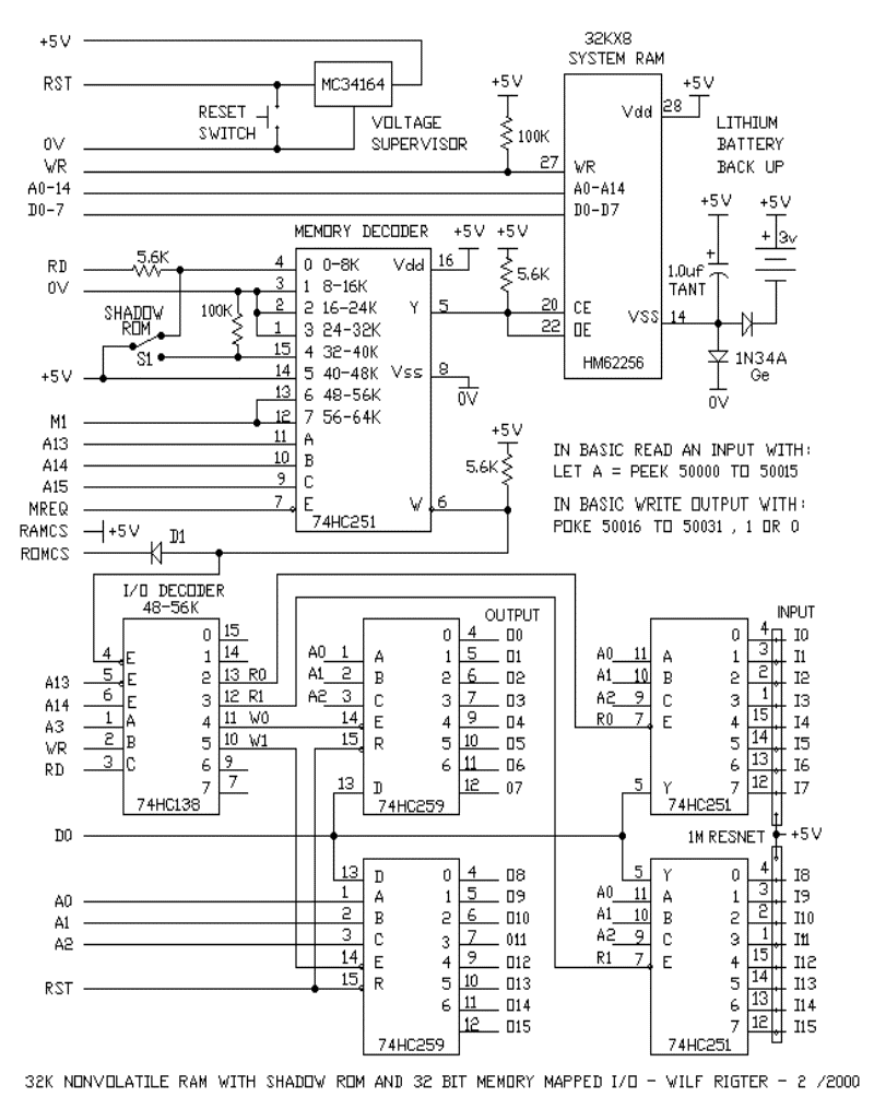
32K RAM plus 32
bit Memory Mapped I/O for the ZX81
Wilf
Rigter ( wrigter@dccnet.com )
Control the World with Peeks and Pokes
This is ZX81 hardware project I designed, build and tested a few years ago but never got around to posting.
It combines a non-volatile 32K RAM design together with memory mapped I/O consisting of 16 input and 16 output lines, that can be peeked and poked in locations 50000 to 50015 (among others). The I/O is bit mapped: reading and writing a single I/O bit at a time at each address location.
The 32K NVRAM
This 32K Byte Static RAM circuit is a simple and powerful upgrade for a stock ZX81/TS1000 and the secret sauce of this design is the 74HC251 MUX used as a memory mapper. A Lithium coin cell provides power to the chip to make the RAM chip contents non-volatile when the ZX81 power is off. While all the RAM contents are nonvolatile, only 8K can be write-protected.
The RAM is allocated in 4 blocks of the 64K memory map controlled by the Z80 CPU. In the Basic memory address space between 16K and 32K, half of the 32K RAM chip is used to replace the conventional 16K RAMPACK (and internal 2K RAM). This part of memory contains in order, the system variables, the Basic program, the Basic Display file, the Basic variables, various scratch pad and temporary memory locations and the machine code stack. This system memory space is tested and initialized by the ZX81 Basic OS on power up and reset and therefore the contents will be erased.
An 8K block of the RAM chip is located between 8K and 16K is reserved for use with popular machine code programs such ZXAS that run from that space, or with high resolution graphics programs such as WRX16 which use that space for the 256x192 bitmapped display file. That space is not initialized on power up but neither is it protected during program execution and during power down from spurious CPU writes. A slide switch (S1) is used to select where the last 8K block of RAM is decoded: in the write protected 0K-8K space, superimposed over the ZX ROM or in the 32K –40K space where the contents of this 8K block are not write protected and can be programmed with new ROM code.
Any code can be installed to run from the 0K to 8K area but the video character pattern tables cannot be changed to give new characters for the ZX display. This is because the old ZX ROM contents continue to be used for normal and pseudo hires patterns. The up side is that the 512 byte memory space between address 7680 and 8191 can now be used for new operating system code without disturbing the video display.
The 32 Bit I/O
The I/O circuit uses a 74HC138 decoder to generate 4 decoded input read enable signals and 4 decoded output write enable signals which can control up to 64 I/O bits. Two read and two write signals are combined with address line A0-A2 to decode 16 input and 16 output bit addresses. The 16 inputs lines use two of the same 74HC251 MUX chips as was used for RAM address mapper. The 16 output lines use two 74HC159 addressable latches. The circuit can be easily expanded to the full 32 input and 32 outputs by adding two more MUX and LATCH chips and using all 8 I/O decoder enable signals.
How the ZXRAM+I/O circuit works
The RAM circuit
The 74HC251 memory decoder chip uses A13-A15 and MREQ to select 1 or 8 inputs. If the selected input pin (0-7) is low, then the output Y at pin 5 is low and the RAM is enabled while the ROM CS line is inhibited. If the selected input pin is high then the RAM is not enabled and ROM line is not inhibited. If the ROM CS signal is not inhibited and A14 is low then a low is generated on the ROM CS line by the ULA and the ROM will be enabled.
The 0V connection to pin 1-3 always enables the RAM chip when those spaces are addressed. The +5V connected to pin 14 disables the RAM chip when 48K –56K space is selected. That will be used later by the I/O decoder to set or reset I/O bits at memory locations 50000-50015.
When the M1 signal connected to pins 12 and 13 is low this enables the RAM chip so that the normal ZX video display can be executed above RAMTOP. For any READ and WRITE memory access to this 48K to 64K address space, the RAM is disabled. This will be used later to install a 512K byte bank switched RAMDISK described in another article.
Finally we come to pin 4 and pin 15 controlled by S1. When S1 is up as shown, connecting pin 4 to 5V, the RAM is disabled in the 0-8K space and the RAM CS line is not inhibited. All access to 0-8K address space then enables the ROM as the ULA generates a low signal on the ROM CS line. As shown pin 15 is connected through a 100K resistor to 0V which means that the RAM is enabled in the 32K–40K address space. This permits the RAM to be programmed with a copy of the ZXROM (shadow ROM) enhanced with various improvements.
When S1 is switched down, RAM in 32K–40K area is no longer accessible (write protected) and that block of RAM is instead switched to the 0-8K area from where the system boots at power up or reset. The Shadow ROM can perhaps be modified for auto running a Basic program from system memory from power up. While the Shadow ROM can execute machine code in the 0-8K space it is write protected and any memory access during RFRSH for video pattern lookup will access the old ROM contents instead.
The I/O circuit
If the ROM CS line is not inhibited by the memory decoder and A14 is high and A13 is low then the I/O decoder is enabled and 1 of 8 of the I/O control lines will be low and enable a read or write of the selected I/O bit. This decoding is enabled for any read or write to the address space between 48K and 56K. A convenient base address in that space is 50000. The A0-2 address lines further decode the I/O address to select 1 of 8 contiguous bit addresses which, combined with 1 of 8 active low I/O output lines, select 1 of 64 I/O bits to PEEK or POKE from Basic.
For example, a Basic program, which reads the logic level at input 03 and applies it to Output 07 would use
10 LET A= PEEK 50003
20 POKE 50007, A
enjoy
wilf