Hello everyone,
In our previous discussion of interfacing an LCD to the ZX81 we used
a 8255 type parallel printer port for generating the data and control
signals for the LCD. This requires 7 or 11 I/O lines depending on the
data width selected. It was apparent from the 8255 MC code listing that
there is a lot of software required to generate the various read/write
data and command control sequences. This makes the LCD less transparent
to use and in practice means LCD software modules are used as black
boxes without realizing the full potential of this LCD.
In the case of a single chip controller like the 16C84, you don't have
any choice but to use I/O ports for interfacing the LCD. However Z80
I/O devices can connect directly to the CPU bus, thereby minimizing
hardware and software complexity. The design is compact enough to
mount it in the original ZX81 case.
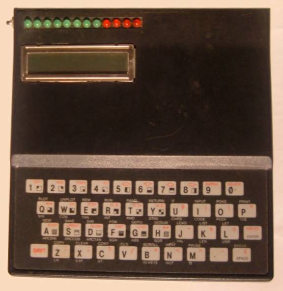
Z80/LCD - A Z80 TO HD44870 LCD INTERFACE
BETA V0.2 OCT 12,1998 BY WILF RIGTER
Here is a design to interface the Hitachi type 44780 LCD directly to
the ZX80 CPU bus. A standard Z80 I/O decoder circuit can not be used
since it does not have the required timing sequence.
By careful design this LCD interface is only slightly more complex
than the standard Z80 I/O decoder. The circuit provides the required
timing for the E signal and adds wait states for interfacing the LCD
to a Z80 CPU bus with a maximum clock of 4 Mhz. The design was tested
on a 3.2 Mhz (ZX81) bus with the following results.
The positive logic E signal requires a minimum 140 ns setup time from
the time WR is stable to the rising edge of E. The circuit insert one
clock cycle delay equal to 300 ns. The address and data lines setup
times are also satisfied.
The minimum duration for the E signal is 450 ns during which all other
signals must be stable. This circuit provides 2 clock cycles or 600 ns.
Finally, the bus signals must have a minimum hold time of at least 10 ns
after the falling edge of the E signal. The circuit provides 1 clock
cycle or 300 ns.
Based on these results this design should perform well with a maximum clock
of 4 Mhz.
The 74HC175 is configured as a moving pulse shift register which
generates the 2 cycle E signal after a one cycle delay.
This circuit also generates a 2 cycle WAIT state pulse ensuring that
the bus signals remain stable for the minimum hold time.
The WAIT signal and the E signals are offset by one clock cycle.
The diode in the WAIT line is only required for the ZX81 but a direct
connection for the WAIT line must be used in all other Z80 applications.
The 74HC138 I/O address decoder would normally be required for other
I/O devices, so the only aditional components for the LCD port are the
74HC175 and 1/6 of a 74HC04 chip.
The advantages of the Z80/LCD circuit include eliminating up to 11 I/O
pins normally used for LCD interface including a bidirectional port and
a greatly simplified programmer model. The less expensive and low power
74HC type parts can result in increased battery life for portable
applications. Don't be deceived by expensive and complicated imitations:)
Some LCD data sheets suggest a Z80 interface design but they use more parts
and do not provide correct timing.
-------------------------------------------------------------------------
74HC138 DECODER
_____
A5-------|A | COMMAND ADDRESS = 0F
A6-------|B | DATA ADDRESS = 1F
A7-------|C |
/M1______|E |
_|/E | 74HC04 INVERTER
/IORQ__|_|/E 0|___|\___
|_____| |/ |
|
| 74HC175 QUAD
D FLIFLOP
5V
______________|_____________
| __|__ __|__
__|__ __|__
|__|D R Q|__|D R Q| _|D
R Q|___|D R Q|__
| | |
| | | | |
| |
| /Q| |
/Q|_| | /Q|_ |
/Q| |
|__C__| |__C__| |__C__| | |__C__| |
CPUCLK___|________|_________|____|____| |
| |
WAIT --->|----------------------+ |
|
D0 D1 D2 D3 D4 D5 D6 D7 | 5V
______|__|__|__|__|__|__|__|______|_______ |
| D0 D1 D2 D3
D4 D5 D6 D7 E Vdd|---+_
/WR______|W/R V0|___| |
10K
A4_______|RS 1x16 LCD (HD44780) Vss|
|_| ADJ
|__________________________________________|----|
0V
Z80/LCD INTERFACE SCHEMATIC
_
_ _w _w _w _
_ _
CLK | |_| |_|
|_| |_| |_| |_| |_| |
_______ _____
/IORQ
|_________________|
_______ _____
R/W
|_________________|
________
______________
/WAIT
|_______|
_______
E ____________| |__________
_________________________
A4(RS)--|_________________________|--
________________________
D0-7 ---|________________________|--
Z80/LCD INTERFACE TIMING
Z80/LCD ASSEMBLY SOURCE
CODE LISTING
Since the hardware takes
care of the timing waveforms,
the assembly source code
for this interface now looks very
simple compared to code
normally used with LCD interfaces.
EXAMPLE Z80/LCD ASSEMBLY
SOURCE CODE
;ZX81 LCD-PRINT STRING
;V0.2 OCT 18,1998
;W.RIGTER
;HD44780 1X16 CHAR LCD
;4 BIT INTERFACE
;ALL DATA IS TRANSFERRED
;IN 2 NIBBLES ON D4-D7
;EXCEPT INITIALIZATION
LCDDATA=1F ;LCD DATA ADDRESS
LCDCTRL=0F ;LCD CONTROL ADDRESS
ENTRY=06 ;INCREMENT/CURS SHIFT
START LD A,30 ;INITCODE IN D4-7
LD B,3
;WRITE FUNCTION 3X
INIT1 CALL DCW ;CMND WRITE WITH
DJNZ INIT1
;DELAY LOOP
INIT2
LD A,20 ;4
BIT MODE SEND
CALL DCW ;IN
1 NIBBLE
;NOW ALL DATA IS SEND IN
;2 NIBBLES PER BYTE
LD A,28 ;4
BIT MODE,2 LINE
CALL CW
;COMMAND WRITE
LD A,08
;DISPLAY OFF
CALL CW
;CMND WRITE
LD A,01
;HOME+CLEAR DSPLY
CALL CW ;CMND
WRITE
LD A,ENTRY
;ENTRY MODE
CALL CW
;CMND WRITE
;END OF INITIALIZATION
LD A,0F
;DSPLY ON,CURSR ON
CALL CW
;COMMAND WRITE
;WRITE 2 STRINGS TO LCD
LD A,80 ;SET
DDRAM ADRS=00
CALL CW
;START OF LINE 1
LD HL,ASC1
;STRING 1
CALL STRNG
LD A,C0 ;SET
DDRAM ADRS=40
CALL CW
;START OF LINE 2
LD HL,ASC2
;STRING 2
STRNG LD A,(HL) ;GET EACH CHAR
INC HL
CP FF
;LAST CHAR
RET Z
;RETURN
CALL DW
;DATA WRITE
JR STRNG
;NEXT CHARACTER
;BUSY/DATA WRITE
DW CALL BUSY ;LCD READY?
OUT LCDDATA,A ;MSB
DATA
RLA
;SHIFT LSB TO MSB
RLA
RLA
RLA
OUT LCDDATA,A ;LSB
DATA
RET
;DELAY/COMMAND WRITE
DCW
PUSH AF
;SAVE COMMAND
LD DE,2000
;DELAY TIME
DCW1 DEC DE ;SOFTWARE LOOP
LD A,D
;TEST FOR DE=00
OR E
JR NZ DCW1 ;IS
DE=00?
POP AF ;GET
COMMAND
OUT LCDCTRL,A ;MSB
ONLY
RET
;BUSY/COMMAND WRITE
CW CALL BUSY ;LCD READY?
OUT LCDCTRL,A ;MSB
COMMAND
RLA
;SHIFT OVER 4 BITS
RLA
RLA
RLA
CW1
OUT LCDCTRL,A
;COMMAND
RET
;TEST BUSY FLAG
BUSY
PUSH AF
;TEMP SAVE AF
BSY1 IN A,LCDCTRL ;RD BUSY FLAG
RLA
;SAVE BS IN CARRY
IN A,LCDCTRL
;NEXT NIBBLE
JR C BSY1
;UNTIL BS = ZERO
POP AF
;RESTORE AF
RET
;ASCII="! ENJOY
- WILF !"
ASC1 21 20 65 6E 6A 6F 79 20 FF
ASC2 B0 20 77 69 6C 66 20 21 FF
END OF LISTING