Foreword
This article is tutorial explaining
how each part of the ZX97LITE works.
I designed the ZX97 as a discrete
copy of the ZX81, which was the first PC for millions of people. In the process ZX97 turned into much more
than a mere copy. While it is backward
compatible with the ZX81, it is in all other respects a significant improvement over the ZX81.
In 1998, Rodney Knaap contacted me to offer to make a PCB of the ZX97 but
this proved no small feat. The end result required 3 PCBs connected together
with flat cables. In order to simplify the PCB for others to build I designed
the ZX97Lite, a trimmed version of the ZX97 omitting the big RAMdIsk and the 8255 parallel port. For a full background on this story and
details of Rodney’s ZX projects , check out Rodney Knaap's
Website where you will also find my original ZX97 article and schematic.
Rodney has designed a single sided
PCB for the ZX97L and also build and tested a prototype using this circuit. I
have been unable to contact Rodney for a long time but I would urge you to try
and contact Rodney for the latest CAD version of the ZX97Lite PCB. If you cannot get in touch with him, here
are the beta version of the ZX97Lite single sided PCB (ZX97LPCB - for 600pdi printer), the
ZX97Lite parts and jumper layout (ZX97Lite Layout ) and my ZX97 EPROM file
(ZX97L 27C256 EPROM binary image)
While Rodney’s ZX97Lite schematic was a great improvement over my original ZX97 ASCII
drawing, it is somewhat difficult to read because of the foreground and
background colors, the dense layout, the bused signal lines, the IEC logic
symbols, crowded pin numbers and in addition, it contains some minor errors and
omissions
In order to make the ZX97L easier
to understand, I have redrawn the schematic by replacing the IEC logic with
ANSI symbols, reformatted the drawing to black on white , renumbered pins and
completed some missing bits. The overall drawing was then “disassembled” into
byte sized smaller functional subsystems.
The eight ZX97L subsystems are the
following:
1) CPU and NOP Circuit
2) RAM and EPROM Memory
3) Memory Decoding
4) CHR$ Decoding
5) Time Base Generator
6) Sync Generator
7) Video Shift Register
8) I/O Ports and External Connector
I like to thank Rodney Knaap for
working the original ASCII schematics of the ZX97LITE into a complete project
together with graphical schematics and an elegant single sided PCB layout way
back when in 1998.
To Jack Raats for encouraging the
work on the original ZX97 and to the rest of all my friends in ZX land:
My warmest regards and enjoy!
Wilf
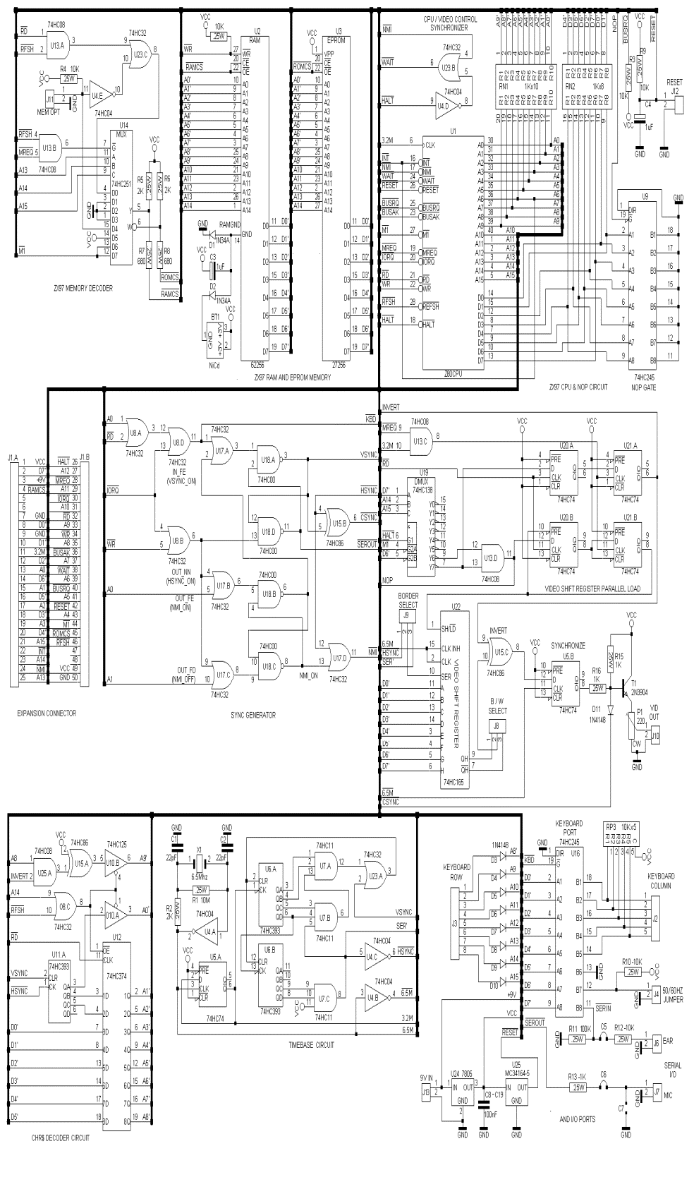
THE ZX97LITE SCHEMATIC DISASSEMBLED Rev. 2.1 - By Wilf Rigter 12 / 2003
The ZX97LITE is a simplified ZX97
designed to fit on one single sided PCB. The ZX97L is a complete ZX81 using discrete
logic chips with 32K of battery backup RAM and 32K of EPROM. User selectable
memory mapping allows the ZX97L to boot directly from user M/C code in RAM. The
circuit draws just 50mA so can easily be run from a battery or even solar
cells. The ZX97L OS supports a bank switched RAM / EPROM disk with a hot key.
The ZX97LITE demonstrates this feature with bundled utility machine code
programs stored in one 16K bank of EPROM DISK. The expanded RAM / EPROM DISK
circuit and the 8255 parallel port of the ZX97 were omitted in order to keep
the PCB layout simple. The ZX97L is virtually identical to the rest of the ZX97
and so this description therefore also applies that original circuit.
1) CPU AND NOP CIRCUIT
The CPU is the subsystem that rules
them all and uses a Z80 inside.
I won't go further into the details of the all Z80 pin functions and CPU
operations as most are used in a conventional manner and information on this is
readily available on the web. But some
of the CPU control lines are used in unconventional ways related to the ZX81
video system and these will be described in detail:
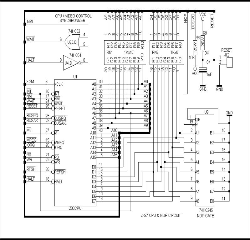
1) The 3.25MHz CPU clock line is
derived from the 6.5MHz video clock after dividing by 2. This is required since
the CPU must load each video pattern byte into the 8-bit Video Shift Register
during a NOP cycle, which takes 4 CPU clock cycles while the 8 pixels are
clocked out of the VSR with 8 video clock pulses.
2) Like the ZX81, the INT input is connected
to A6. The Z80 decrements the refresh address counter and the INT input is
sampled during RFSH time for an active low on A6 to interrupt the HALT
condition. That HALT state occurs at the end of each normal SINCLAIR video
line.
3) The NMI line and NMI service
routine at ROM address 0066 is used in SLOW mode to interrupt user program
execution during blank video lines to switch to video display or VSYNC
execution when required. The NMI generator is controlled with OUT FE = NMI ON
and OUT FD= NMI OFF to gate the HSYNC signal from the Time Base Generator to
the CPU NMI input.
4) The WAIT line is used to finely
synchronize the Z80 with NMI timing twice during each video frame with the
NMI–CONT service routine at ROM address 02A9.
The HALT and NMI lines decoded with an OR gate and inverter just like
the ZX81 used a transistor and some passive parts to do this.
5) When active during the live
video mode, the NOP generator (U9) forces a NOP (00) code on the CPU D0-D7 data
lines while the CHR$ code is loaded into the CHR$ decoder circuit. During RFSH,
the A0’-A9’ lines address the video pattern byte in EPROM or RAM to be loaded
into the video shift register
6) During forced NOP, the eight
resistors in RN2 isolate the Z80 D0-D7 data lines from the D0'-D7' data lines
used in the rest of the ZX97L system. At all other times D0'-D7' transfer data
between the Z80, memory and I/O ports.
7) The ten resistors in RN1 isolate
the Z80 A0-A9 address lines from the A0'-A9' address lines used in the rest of
the ZX97L system. The A0'-A9' address
lines are normally used by the Z80 to address memory and I/O. During live video
RFSH time, the CHR$ decoder circuit supplies the address to the A0'-A9' lines
for a video pattern byte in RAM or EPROM.
a) A0'-A2' = video character line
counter (character height = 8 lines)
b) A3'-A8' = CHR$ code
c) A9' = invert video or select second character set
9) The RESET line, connected to
R9/C4, initializes the CPU on power up. A voltage supervisor discussed in part
8 is also connected to this line and J12 is used for connecting an external
reset pushbutton.
2) RAM AND EPROM MEMORY
The original unexpanded ZX81 had 1K
of static RAM and an 8K ROM for the ZX81 BASIC operating system. The RAM contains the system variables, BASIC
and M/C programs, BASIC variables and the Z80 stack.
One interesting side effect of
using a 1K ZX81 is that the RAM can barely contain the 24 x32 character video
display file (DFILE) before running out of memory for the other RAM
contents. To deal with that 1K
limitation, the ZX81 DFILE is
compressed to just 24 bytes of carriage returns or New Line (N/L) characters at
system initialization and after a CLS. As characters are displayed on the
screen each video line is expanded as required. Up to 32 displayable characters can precede the N/L character.
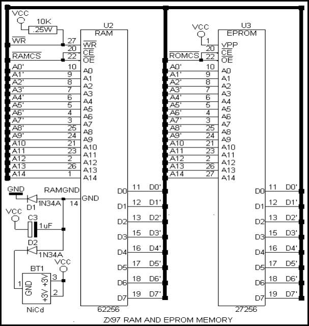
As an indication of how tightly the
CPU is coupled to display of the ZX81 video consider the following:
The N/L CHR$(118) at the end of
each of the 24 DFILE character lines is actually a HALT opcode. In effect,
displaying a N/L character caused the Z80 to HALT. The Z80 INT line connected
to A6 (a mentioned in part 1) wakes up the halted CPU at the end of each
horizontal display line before updating the parameters for the next horizontal
video line.
The ZX97L uses a low power CMOS
32Kbyte Static RAM chip with battery backup power for protecting the RAM
contents during power down. The 32K EPROM contains the ZX81 OS modified to
include several new BASIC keywords for direct access to the included RAMDOS
directory program and the included machine code assembler and disassembler
programs located in the upper 16K bank of EPROM memory. This upper 16K area is the area where the ZX97L can be expanded
with a bank switch, which will provide up to 32 pages of 16K each (512K
total) like the original ZX97.
The memory subsystem shows the
simple battery backup system for the CMOS RAM using a 3V lithium coin battery
and some diodes. The common Vcc
connection instead of common GND has the advantage that all lines connected to
the RAM are automatically pulled up to Vcc (rather than GND) during power down.
There are two resistors elsewhere in the circuit that pull up the tristate
RAMCS and ROMCS lines. An additional 10K pull up resistor on the RAM /WR line
as shown in the schematic is highly recommended to protect the RAM contents
during power down.
Many Z80 systems use RD connected
to the memory chip OE lines. In the ZX81 OE and CE are connected together so that
memory contents can be read during RD and RFSH time when the video pattern are
fetched.
After this little warm up exercise
with the simple CPU and memory circuits, we examine how the ZX97L uses a memory
mapping circuit to decode the 32K of RAM and 32K of EPROM memory into various
8K blocks in the 64K memory space.
3) MEMORY DECODER
While reverse engineering the ZX81
ULA, I used the ZX80 circuit as a guide since the ZX81 ULA chip circuit
operation and the ZX81 ROM were backward compatible with the older ZX80 and so
had to be designed similarly. The main difference in the circuits was the ZX81
ability for SLOW mode video operation. My objective for the ZX97L was to create
a discrete TTL ZX81 with increased functionality that used fewer parts than the
ZX80 and was a transparent circuit design so that its operation could be
understood by anyone with some experience in TTL logic circuits.
The ZX80/81 had a primitive memory
decoding circuit, which used MREQ together with /A4 and A14 to generate the
ROMCS and RAMCS lines respectively. As a result, copies of the unexpanded ZX81
RAM and ROM memory images were echoed at intervals throughout the 64K memory
space. This was corrected in many memory add on devices which included more
complete decoding of the memory by overriding the ZX81 RAMCS / ROMCS signal
lines. The ZX97L memory mapping circuit may generate the same RAMCS and ROMCS
signals but in every other respect this decoder is anything but primitive.
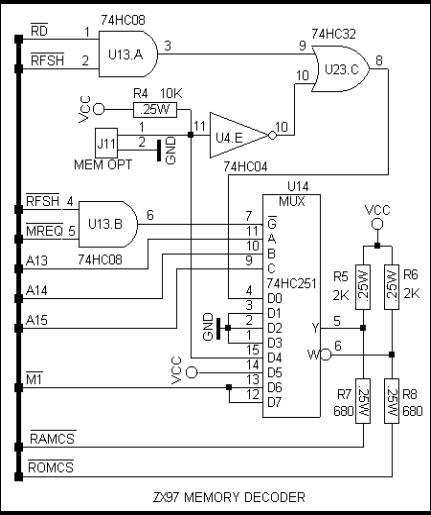
The decoder circuit uses a 74HC251
MUX (U14) to generate the EPROM and RAM chip select (CS) signals. These 32K
memory chips are decoded into a patchwork of 8K memory blocks mapped in the Z80
64K memory space.
The ZX97L memory is mapped out as
follows:
0-8K = EPROM or RAM - the ZX97L
BASIC firmware in EPROM or the BASIC
firmware with enhancements in write
protected RAM.
8-16K = RAM - machine code
programs, second video dot pattern lookup table, etc.
16-32K = RAM - ZX81 BASIC program
memory just like an expanded ZX81 with 16K RAM
32-40K = RAM or EPROM - 0- 8K
Shadow RAM or ZX97L OS in EPROM.
40-48K = EPROM - machine code
programs, Hires files, etc.
48-64K = EPROM or RAM - 16K
EPROMDISK and DFILE echo in RAM (no machine code program execution allowed) or
future 512K RAMDISK.
The 74HC251 MUX (U14) uses the
A13-A15 address lines together with an active low enable from the U13.B output
to select one of the D0-D7 data inputs. When the inputs of U13.B (/RFSH or
/MREQ) are both high, the Y and W outputs of U14 are tri-stated and R5 and R6
pull the two memory select lines to Vcc.
If either input pin of U13.B (RFSH
or MREQ) is low, the MUX is enabled and if the selected data input is low then
the RAMCS is active low or if the selected data input is HIGH then the ROMCS is
active low. When the MUX is enabled by
U13.B, the 64K memory map is translated as follows:
1) To take a simple case first with
input D1 selected and connected to GND, the 8-16K-memory block is enabled in
RAM. This area is traditionally used to run machine code programs like the ZXA
assembler. Several utility MC programs are bundled in the 16K EPROM disk. The
RAMDOS directory program, using the new keyword DIR that can be used in BASIC
programs, lists, loads and runs these MC program files in the 8-16K RAM area.
2) With the D2 and D3 inputs
selected and connected to GND, RAMCS is generated which enables 16K of RAM from
16K-32K for the ZX81 BASIC system, DFILE and user BASIC programs. This 16K
block of RAM is just like a ZX81with a
16K RAM pack attached
3) With input D5 selected and
connected to Vcc, selecting the memory block between 40K- 48K always generates
ROMCS to map EPROM in that area which is used to store and run additional firmware or video pattern tables.
4) The D6 and D7 inputs are
connected to /M1 which makes it a little more complex case:
The memory mapper circuit uses /M1,
which is active low when machine code is executed, to differentiate between video
and EPROM memory access. The ZX81 reserves the 48-64K area for the execution of
ZX81 video display file (DFILE) or rather an echo of the DFILE 16-32K area.
When /M1 is active, D6-7 inputs are low, RAM CS is active and an echo of RAM in
16-32K is enabled. Since MC program execution is reserved to the processing the
ZX video display file echoed in this 16K memory space, direct access to the
48-64K area is restricted to storing data files and no machine code can be
executed. For the unexpanded ZX97L, when
/RD or /WR are active, the D6-7 inputs are high and the ROMCS output is active
to enable the upper 16K of the system 27C256 EPROM. or (future) bank switched
pages. In a sense, the allocation of the 48-64K memory as either RAM or EPROM
is changed on the fly by the /M1 signal.
5) The D0 input logic is the most
complex case. The first 8K block is used like the classic ZX81 ROM with the
ZX81 BASIC operating system but can be swapped with user enhanced OS in Shadow
RAM. This is great for OS development when testing new code. For example, new
video patterns can be added or fast communication routines can replace the ZX
tape routines. The decoder MUX D0 input is controlled by J11, which is also
connected directly to D4. When D4 is high ROMCS is selected and when D4 is low
RAMCS is selected. With J11 closed, the inverter U4.E output and U23.C OR gate
output, connected to D0, is high and the 0-8K EPROM block, with the ZX81 OS, is
enabled in 0-8K of the memory map . With J11 open, the EPROM ZX OS is swapped
with an 8K RAM page which normally resides in the 32-40K area but which can be
loaded with new or modified operating system firmware.
The U13.A AND gate is used to
access the 0-8K in RAM only if /RD or /RFSH
are low to write protect RAM in the
0-8K area. This is an important consideration since several ZX81 OS operations
routinely write to memory in the 0-8K area
(let alone a runaway program randomly overwriting the OS in RAM)
After this relatively complex
subsystem, we are ready to test our ZX-IQ on the circuit that converts the ZX81
alphanumeric and graphic CHR$ codes into video patterns to be displayed on the
monitor screen with some small but significant improvements over Sir Clive's
design.
4) CHR$ DECODER
This subsystem is closely tied to
the ZX81 video design, which has mystified more than a few experienced ZX81
fans. By following along with the description of operation of this circuit, we
learn much about the clever ZX81 video system and discover that Sir Clive missed
some powerful video options for the ZX81 by just a few extra gates.
The ZX81 alphanumeric and graphic
characters in the video display file (DFILE) consist of up to 768 (24x32) bytes
of CHR$ codes. These are converted into rasterized patterns of video pixels and
displayed on the monitor screen as 32 blocks of 8 x 8 light or dark pixels. For
each of the 64 displayable ZX81
character codes, a rasterized graphic shape is stored in 8 contiguous bytes in
a video dot pattern lookup table in the last 512 bytes of the 0-8K ZX81 ROM.

The CHR$ decoder operates in two
steps:
1) The Z80 reads each character in
DFILE and together with the CHR$ lookup circuit generates the address of a dot
pattern byte
2) The dot pattern byte is accessed
during RFSH and loaded into the video shift register to be shifted out serially
at 6.5M pixels per second.
The DFILE echo above 32K is
literally "executed" during the video display. Each CHR$ in the DFILE
is fetched by the Z80 as an OPCODE , but executed as a NOP instruction during 4
CPU clock cycles. The CHR$ decoder circuit uses 6 bits of each fetched CHR$
code together with 3 bits of a the horizontal line counter and with part of the
Z80 RFSH address to form the address to a byte in the dot pattern lookup table.
The three bits of line counter
U11.A, which is clocked by each HSYNC pulse, are used for A0'-A2'of the pattern
byte address. The counter increments 8 times as each row of DFILE characters is
read 8 times in succession. This generates one row of video characters on the
screen, with each adjacent character made up of 8 bytes of video dot pattern
data in a block of pixels 8 high by 8 wide. This is repeated for each of the 24
character rows. The total number of controlled dots (screen resolution) for a
ZX81 screen is 256x192. The lower 6 bits of each CHR$ code in DFILE is clocked
into U12 at the end of the /RD signal and makes up A3'- A8' of the video
pattern look up address. The CHR$ D6-7 bits are used, in the VIDEO circuit,
discussed later in PART 6, to enable video and to invert the video pattern for
that CHR$, generating a reverse foreground - background character on the
screen.
These 9 least significant address
bits (LSB) select one of the 512 video dot pattern bytes. are stored and tristate isolated with U12 -
(octal register) and U10.A (tristate buffer) until the RFSH and A14 are both
low which then enables 9 LSB on the A0'-A8' address lines. The most significant
7 address bits of the dot pattern byte address are supplied by contents of the
Z80 Interrupt Register (IREG), which is gated onto the A8-A15 lines during RFSH
time. The 7 bits in the I register are therefore used to point to the start of
the lookup table while 9 least significant address bits (LSB) select one of the
512 video dot pattern bytes in that lookup table.
So far this circuit functions similar to the ZX81 ULA circuit but
with one significant difference:
1) In the ZX81, the pattern lookup
table must be in the internal ROM because the ULA CHR$ decoder A0'- A8' outputs
lines are physically connected to the only to the ROM address lines.
2) In the ZX97L CHR$ decoder both
the RAM and ROM can be accessed and either can be used for the pattern lookup
tables as long as they are located in 0-16K or 32-48K (ie A14 low). This was
done to permit the display of true hires video which requires that CHR$
decoding is disabled and means that hires display files must be located in
16-32K or 48-64K. Given that limitation, you can locate one or more user
defined 512 byte pattern lookup tables in RAM for example in the 8-16K or 32-
40K area. The first byte of the lookup table must be located on a 512-byte
boundary (ie locate the table between 8192 - 8703).
All that is needed to access the
new lookup table is to load the IREG with the high order 7 bits of the table
starting address. Note that bit D0 of IREG (gated to the Z80 A8 line but not to
the A8' line) is normally 0 but is otherwise ignored in the ZX81 CHR$ video
mode.
A second enhancement provided by
the ZX97L CHR$ decoder circuit gives you a choice of using 64 Characters and
their reverse in a 512 byte pattern table or 128 unique characters in a 1024
byte pattern table. In the normal ZX81
CHR$ video mode there are 64 CHR$ codes with unique patterns stored in a 512
byte pattern table and uses CHR$ bit D7 to invert video for that CHR$,
generating the same pattern but with reversed foreground / background colors on
the screen. The details of the shift register and the parallel loading pulses
are described in the ZX97L Video Circuit.
In the ZX97L enhanced CHR$ video
mode D7 of the CHR$ code is combined with D0 of IREG to address a second
pattern table thereby doubling the number of unique displayable characters to
128 instead the normal reversed character set.
For example, both upper and
lowercase alphabet characters as a well as new symbols or new graphic game
characters can be displayed. This second table of 64 character video patterns
can be located for example in 8192-8703 RAM, contiguous with the existing ZX81
video pattern table in 7680-8191 EPROM.
To enable the 128 CHR$ mode, set
bit D0 of the IREG to a logic 1. Now instead of simply reversing the displayed
character whenever D7 of the CHR$ code is high, a second unique pattern (ie
lowercase) for that CHR$ is displayed. Bit D0 of IREG and D7 of the CHR$
generate A8 and INVERT at the inputs of AND gate U25.A at RFSH time. If INVERT
and A8 are HIGH, the U25.A output A9' is high and accesses the second pattern
table.
Note that dot patterns in the
second pattern table are displayed in reverse video but that is simple to
correct by loading the second table with reversed (instead of normal) dot
pattern bytes.
The Time-base Generator is next. (It's
a much simpler circuit to give us all a bit of a break).
5) TIME BASE GENERATOR
Compared to the convoluted
"CHR$ to video" circuit, the ZX97L time base circuit has a certain
clarity. The circuit consists of a
6.5MHz CMOS crystal oscillator, which
is the clock for the video shift register. The 6.5M signal is inverted with
U4.B. to generate the /6.5MHz signal. A
divide-by-2 D flip-flop (U5.A) generates the 3.25MHz CPU clock. A divide-by-207
(U6+U7) circuit generates the 15,750kHz video horizontal sync pulses.
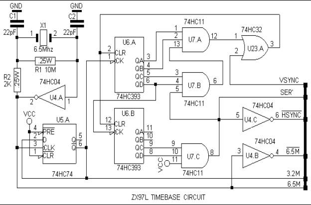
The HSYNC pulses occur between each
horizontal video line and are used by the TV/monitor to synchronize the video
dot stream with the start of the electron beam scanning the next horizontal
line across the phosphor screen of the TV/monitor.
The HSYNC divider consists of 8
binary counter stages (U6). Three 3
input AND gates decode the binary count of 11001111 (208 decimal) to reset the
counters to zero. The last two divider stages are connected to AND gate (U7.C)
which generates the actual HSYNC pulse. The HSYNC pulse width is 15/3.25= 4.6
usec and horizontal line duration is 207/3.25=63.7 usec.
There are 192 lines used to display
the 24 rows of video characters. The (50/60Hz) vertical sync frequency is
selected depending on a jumper setting (J4), which is described later. With a
60Hz Sync there are 262 lines total generated per vertical field and with 50Hz
there are 313 lines per field. Since 192 lines are used for video display, the
remaining lines are blank lines during which slow mode program execution takes
place. As a result, the 50Hz slow mode user program execution speed is almost 2
times faster than the 60Hz setting.
During slow mode program execution,
the HSYNC signal is gated to the Z80 NMI input and interrupts the user program
every 64 usec. The NMI service routine counts remaining blank lines on the
bottom of the screen until VSYNC must be generated and then counts the blank
lines at the top of the screen until the live video display must be generated.
The HSYNC “divide by 207” circuit is synchronized with the VSYNC pulses by
holding the counter reset via U23.A when the VSYNC output is active high.
By now you may wonder how useful
this rather specialized information is? Well the easiest way to a better
understanding of the ZX80 and ZX81 (which I'm sure everyone here has an
interest in) is through the ZX97L, which in part was designed for just that
purpose. The ZX97L circuit was also used as a model of the ZX81 ULA as discussed
in the extended correspondence I had with Carlo Delhez during the development
of his very fine XT2 emulator.
6) VSYNC / NMI CIRCUIT
This part of the ZX97L will look
familiar if you have ever looked at a ZX80 schematic. I tried to simplify it
but could not without losing the transparency of logic, which makes this
subsystem almost self-explanatory.
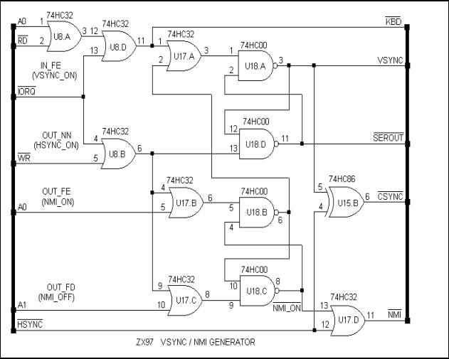
The circuit consists on an I/O
address decoder and two R-S latches (U18). The decoder uses U8 and U17 to
decode the following I/O addresses defined in the ZX81 operating system:
IN FE - Read keyboard port and Start Vertical Sync
OUT nn - End Vertical Sync (any I/O write - no specific address)
OUT FE - Turn NMI pulses on
OUT FD - Turn NMI pulses off
In addition, IN FE reads the keyboard
anytime but to start Sync, the NMI pulses must be off (ie in the FAST
mode).
The 256 I/O addresses are not fully
decoded as the circuit uses the same linear decoding as the ZX81 with each
address bit reserved to a RD or WR I/O address. That means that the hardware
will respond to any I/O address wit
A0 or A1 low but addresses FE and
FD are normally used for the sake of consistency with existing ZX81 software.
Throughout the remaining
description the terms set and reset refer to forcing the state of the S-R latch
outputs, which are used to generate various output signal.
IN FE
An active low on IORQ, RD and A0
generates the keyboard enable signal, which
will be discussed later together with the ZX97L keyboard port. Reading
I/O address FE also sets the Vertical Sync pulse but only if the NMI latch is
off. That way a M/C program can read the keyboard port directly without
disturbing the video if the ZX97L is in the SLOW mode.
Also note that the ZX81 uses the
VSYNC latch to modulate the ULA video output pin with the tape output (mic)
signal. That is what causes the familiar striped signal on the screen during
tape saving and loading and also saved a precious I/O pin on the ULA. However this mixed use of the video pin also
means the HSYNC signal is mixed in with the tape signal making that port
difficult to use for direct serial communication.
The ZX97L has no such constraints
on I/O pins, so the SEROUT output is separate from the video output, not
affected by the HSYNC signal and can be reliably used as an asynchronous serial
transmitter (“bit banger”) output.
OUT nn
An active low on IORQ and WR at any address (usually OUT
FF) resets the Vertical Sync pulse.
This may seem primitive but is required to conform with various ZX81 video
drivers (normal and hires) some of which use the IORQ WR generated during the INT acknowledge cycle
to reset the sync pulse.
As described in IN FE , this signal
is also used to generate the tape or serial output pulses.
OUT FE
An active low on IORQ, WR and A1
sets the NMI latch. The NMI latch
controls U17.D which gates HSYNC pulses to the Z80 NMI input. When the NMI
latch is turned on, the ZX97L is in the slow mode and program execution only
occurs when the video is not being serviced. The NMI pulses interrupt the user program execution every 64 usec, CALL the NMI service routine
to decrement a blank line counter and either returns to the user program or
executes the video routines VSYNC and DISPLAY) if required.
OUT FD
An active low on IORQ, WR and A1
resets the NMI latch and blocks the NMI
pulses. This occurs when the ZX97L fast mode is desired, for VSYNC, for
tape
load and save (serial i/o) and
during execution of the video routines. CSYNC
The horizontal and vertical sync
signals are combined in the XOR gate U15.B Keep in mind that the active VSYNC
signal disables the HSYNC counter and
therefore the output of U15.B generates an active low OR composite sync
(CSYNC) signal, which is combined with the video dot pattern.
7) VIDEO SHIFT REGISTER
This part of the ZX97L was probably
the most difficult to design in terms of generating the precise timing to get a
stable video image on the screen. Many parts of the ZX97L hardware, CPU and
software must smoothly work together to generate the video display. This part
combines that effort in the composite video output to the TV/Monitor.
DFILE ECHO DECODER
The basis of the ZX81 video display
system is the execution of an echo of the
DFILE characters during which the Z80 is forced to execute NOP instructions.
This video circuit uses a special
DFILE echo address decoder (U19), which provides an output (NOP) when the
displayable characters of DFILE are executed in the upper 16K of memory. The 74HC138 octal decoder (U19) inputs C, B
and A are connected to the A14, A15 address lines as well as CHR$ data bit D7
that identifies an inverted dot pattern. The M1, CHR$ data bit D6 and HALT
signals are connected to the chip enable lines.
As a result, the decoder generates
two valid active low output states: Y6 or Y7, which represent non-inverted and
inverted video data. When low, the Z80 ALT signal disables the decoder as the
last character (N/L) of a horizontal
line is executed and the CPU enters the
HALT state executing NOPs until the INT line goes active low and the HALT state is exited.
The active low signals on Y6 and Y7
are OR'd with U13.D. The active low NOP signal at the output of U13.D is used
to enable the NOP generator described in the CPU part. The NOP generator fools
the Z80 into executing NOP instructions while the CHR$ data in DFILE is
converted into a dot pattern byte to be loaded into U22, the video shift
register (VSR).
Note that except for video
execution, DFILE is not otherwise accessible in 48K-64K. Also note that this
video decoding means no M/C program code can be executed in 48K-64K, which is
therefore only used as a Silicon Disk space for file storage.
The VSR is loaded asynchronously
through the parallel inputs with an active low load pulse generated from the
NOP signal delayed by U20.B and U21.B. The load pulse is clocked out on /Q of
U21.B at the end of the last T state of the RFSH cycle, which is decoded with
U13.C. The load pulse duration is just a few tens of nanoseconds of propagation
delay thanks to the connection between /Q of U21.B and the U20.B preset
input. The VSR load pulses, the VSR
data and the invert signal are resynchronized with the (inverted) /6.5M video
clock using U5.B to ensure a crisp and seamless appearance of the dot patterns
on the screen. The ZX80 used some RC components in a kludge circuit to
accomplish the same load pulse shaping.
These are generally unstable and the video quality may deteriorate with
time and temperature.
THE INVERT CIRCUIT
The Y7 output (decoded D7 bit of
the CHR$ code) is delayed and latched
(U20.A and U21.A) when the VSR is loaded and if high, XOR gate U15.C
inverts the serial dot pattern as it is clocked out of the VSR. This INVERT signal is also used in
conjunction with the Z80 I register to select the second character pattern
lookup table.
BLACK ON WHITE ON BLACK
The foreground and background
colors (B/W) of the display and the borders around the display are user
selected with J8 and J9.
VIDEO OUTPUT
The video signal is combined with
the composite sync signal using resistors R15-16 and D11. The summed signals
are buffered by T1 and the VID output level is adjusted with P1. The video
signal has three distinct output levels, from most positive to GND: white, black and sync
HINDSIGHT
The design of the load pulse
circuit came before the addition of U15.C, which reduces the stringent timing
by re-synchronizing the combined VSR data with the inverted video clock. Some simplification could be made to reduce
the ZX97L chip count by one.
For a more intimate look at the
ZX97L and ZX81 video timing details also read the ZX81 video tutorial.
8) I/O, POWER SUPPLY AND EXPANSION CONNECTOR
This is the last and simplest part
of our ZX97L circuit disassembly and potentially the most interesting because
it interfaces with signals from the
outside world.
EXPANSION CONNECTOR
Rodney's schematic shows two 25-pin
connectors (J1A,J1B), which are the equivalent of the 46-pin edge connector of
the ZX81. These pin connectors are lined up side-by-side in dual row header,
compatible with a 50 pin insulation
displacement connectors on a flat cable that can be terminated with a 0.1 inch
edge connector to connect to ZX81 peripherals. The order of the signals seems
to be mixed up in the schematic but looks ok in the component layout but this
needs to be confirmed.
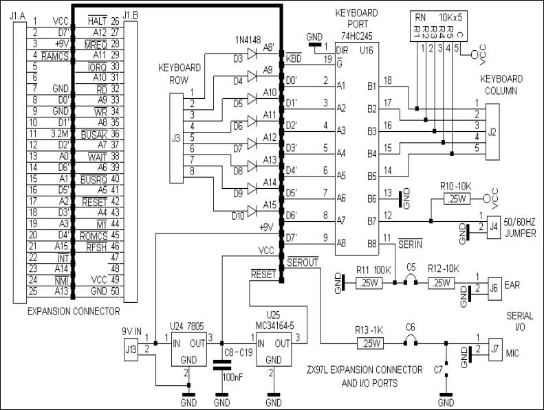
5V VOLTAGE REGULATOR
The 7805 is a standard 5V/1AMP
linear voltage regulator for the Vcc power supply. A better choice is a LM2930
- 5V/150mA low dropout voltage regulator allowing the use of a 6V battery
instead of an 8V minimum unregulated input supply voltage. The LM2930 regulated
ZX97L circuit uses 50mA, which would leave 5V/100mA for peripherals.
UNDERVOLTAGE RESET SUPERVISOR
The MC34164 is a simple way to
protect the memory contents from power-up and power-down transients. The
supervisory chip comes in a TO92 transistor type package. The chip output pin
holds the reset line low until the voltage at the input (Vcc) is greater than
4.5V.
INPUT PORT
The ZX97L has an 8 bit input port
mapped at I/O address FE of which 5 bits (D0-D4) are used for the keyboard
column data, one bit (D6) for 50/60Hz select and 1 bit (D7)
for tape or serial input. The 8th
bit (D5) is not used.
KEYBOARD
The keyboard is made up of 8 rows
of 5 keys. Each row of keys has a common connection for the 5 pushbutton switch
contacts. That common of each row is connected to J3 and is scanned by an
address line (A8-A15) from the Z80 isolated with a diode (D3-D10). The other
side of each row of five switch contacts is connected to J2, with the 5
keyboard columns on U16 - D0-D4. These keyboard column inputs are pulled up
with 10K resistors in RP3 (not shown in Rodney’s schematic). By reading the
keyboard (IN FE) with one of the 8 address lines low, the keys for that row are
read in. Repeated times 8 and all keys of the keyboard are read in by the OS
software.
50Hz/60Hz
This input D6 is read by the OS and
the number of blank lines above and below the live video display is determined
based on the jumper setting.
SERIAL IN / SERIAL OUT
Bit D7 of U19 is used here for
SERIN, a logic level equivalent of the ZX81 ape input, which can be driven, for
example, by a PC parallel port or another ZX97L. The ZXTAPE software is a
simple PC program can be used to send ZX81 files from the PC to the ZX97L using
the same protocol as the ZX81 tape LOAD signal at a rate of about 100 bits per
second in the FAST MODE.
Similarly the SEROUT line is left as a logic level signal
compatible with the SERIN line and two ZX97Ls can connected back to back to directly
exchange information using the BASIC LOAD and SAVE commands. This arrangement
is a change from the ZX81 and from Rodney's ZX97L PCB layout, which have tape
recorder compatible input and output circuits. The logic level version uses
fewer parts and has some changed component value. ZX purists may wish to
install the additional components to make these lines tape compatible.
CONCLUSION
The ZX97L is a minimal but highly
functional BASIC computer with hardware and software that is compatible with the
ZX81. The simplicity of the design makes the logic easy to understand and
useful as an educational aid while the low power consumption and video output
makes it practical for some portable applications.
Next
some ZX97L additions - a 512K byte
memory expansion and an 8255 for
printing,
high-speed communication with a PC and controlling the world.
The complete
ZX97 schematic Redrawn By Wilf Rigter 12 / 2003