IMPROVED ZX81
WAIT CIRCUIT Rev 2
07/2005 - wilf rigter
Ever wondered about the purpose of TR1 in the ZX81 schematic? TR1 together with some passive parts are connected to the CPU WAIT,NMI and HALT lines and generates WAIT states when a NMI pulse occurs. Ok, but why generate WAIT states? The short answer is to synchronize the CPU to VIDEO timing. Still interested? Then read on to understand exactly why and how this circuit works and how, with a small hardware mod, we finally correct a bug to let us execute slow mode user programs10% faster (about a quarter century too late). First note that this TR1 circuit is not needed for FAST mode video, which is entirely generated in software with an overall fixed execution time. In the SLOW mode, the video display is interleaved with user program execution during blank lines at the top and bottom of the screen. The NMI generator is used to periodically interrupt the user programto determine if it is time to service the video. The CPU response to the NMIpulse can have a latency (and jitter) of up to 23 clock cycles depending on which opcode is interrupted. During user program execution, this jitter does not affect video timing of the blank lines which is controlled by the horizontal sync pulses generated by the NMI hardware in the ULA. When the time comes to generate the video characters on the screen or generate the vertical sync pulse then this NMI response jitter must be eliminated. This is done when the NMI routine jumps to the NMI CONT routine, executes theHALT at address 0079 and then waits for one more NMI pulse to exit the HALT state. NMI CONTINUED SUBROUTINE 006F EX AF,AF' ;retrieve main register AF0070 PUSH AF ;now save all application 0071 PUSH BC ;program registers0072 PUSH DE0073 PUSH HL0074 LD HL,(DFILE) ;needed only if IX=0281 and0077 SET 7,H ;if DFILE is executed0079 HALT ;CPU T state/video synchronization 007A OUT FD,A ;turn off NMI generator007C JP (IX) ;to VIDEO-1 or VIDEO-2 However there is a problem: while halted, the HALT opcode executes NOPs every4 clock cycles (T1-T4) and it can be at any clock cycle when NMI arrives but does not respond to NMI until the rising edge of the T4 state. This means HALT itselfhas a latency of up to 4 clock cycles before it exits the HALT state at T4 in responseto the NMI pulse. So what is so important about 4 clock cycle jitter? The problem is that ZX81 SLOW mode video is displayed by executing NOP instructions. The execution time of a NOP is 4 clock cycles which is the time it takes to clock out 1 byte of pixel data but the loading of that byte into the video registermust occur on a specific edge of 1 of those 4 clock cycles to avoid jitter of the video display screen. Since this part of the video is under real time CPU control, the CPUmust be internally synchronized to one edge of a specific clock cycle at the rising edge of NMI to ensure that each displayed video frame starts in exactly the sameplace on the screen. To do this the TR1 circuit was added that acts like an OR gate with an active low WAIT output at the collector of TR1 when NMI is low and HALT is high. 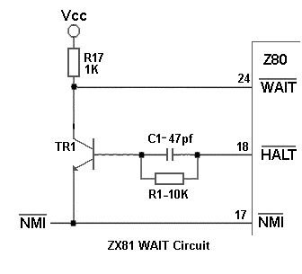
The WAIT state is asserted after the HALT line goes high when NMI forces theHALT exit, and inserts WAIT state betweens T2 and T3 of the M1 cycle of theNMI response (RST to 0066) for the duration of the NMI pulse. Then on the rising edge of NMI, the WAIT signal is removed and the CPU is precisely synchronized with the start of T3 on the rising edge of the NMI pulse eliminatingall video jitter. While the original WAIT circuit solves one problem it comes at a price: The WAIT line is also asserted by every NMI pulse during blank line user programexecution and this reduces available CPU time by 10 %! An improved WAIT circuit adds just one 10K resistor (R35) and PNP transistor(TR3) circuit to correct this problem and increases SLOW mode program speed by 10%. TR1 and TR3 form a LATCH, which is SET on the rising edge ofHALT and RESET when the NMI pulse goes high again. 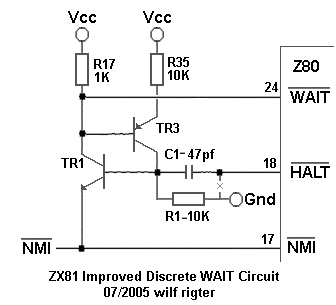
The new WAIT circuit only generates WAIT states when synchronizing the CPU with NMI after the exit of HALT at address 0079. Since that occurs just twice during each ZX81 video screen display there is no time wasted in generating unnecessary WAIT states during user program execution. With a few tools and modest soldering skills, installing this mod is a simple andpainless procedure which took me 10 minutes to complete. The lead of R1 to Z80 pin 18 is first unsoldered from the PCB pad and then soldered to Ground. Then TR3 and R35 are soldered to the original WAIT circuit as shown here: WAIT MOD OF ZX81 PCB ISSUE ONE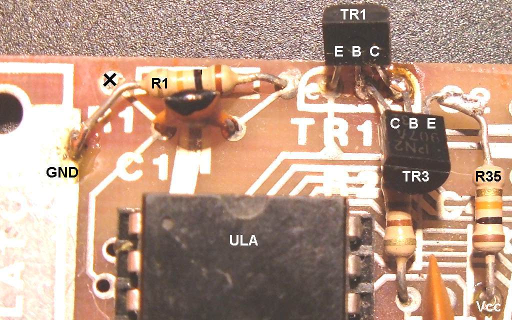
So with a few hints and few pennies worth of parts, the ZX81 could have beenrunning on all cylinders. We can only imaging the millions of MIPS wasted by the old WAIT circuit. The question is now whose head(s) should roll? enjoy wilf