A VERSATILE 64K RAMPACK FOR THE ZX81
24/04/2005 - wilf rigter
Memory decoding on a ZX81 is both simpler and more complex than you think.
The ZX81 uses the simplest memory decoding possible with the ULA generating two decoded memory enable lines ROMCS (/MREQ plus /A14) and RAMCS (/MREQ plus A14) which are mutually exclusive (never active at the same time). These signals each have a 680 ohm resistor in series with the ULA pins and are connected to the ZX81 ROM and RAM Chip Select pins.
Within the available 64K memory map, these two signals each control 32K of non-overlapping memory space in two 16K blocks (ROMCS=0-16K, 32-48K , RAMCS = 16-32K, 48 –64K).
If internal RAM and ROM chips were each 32K bytes in size then the memory map would be fully decoded (no echos).
However the ZX81 ROM is only 8K this means that the same ROM chip can be accesses in 4 x 8K locations in the memory map: 0-8K, 8-16K, 32-40K,40-48K containing the same ROM contents and are therefore referred to as "echos". The primary location of the ROM is 0-8K because that is where the ZX ROM program is executed and all absolute memory references are to that location.
Depending on the size of the RAM chip there are multiple echos. For a 1K ZX81, there 32 echos of the 1K RAM contents that dot the memory landscape. For a 2K TS1000, there are 16 echos. The lowest echo in memory is
the primary location for RAM.
Now comes the first of the tricky parts:
The ULA ROMCS and RAMCS signals are connected to the internal memory chips and are also brought out on the ZX rear edge connector but not to control external memory. Instead it is the external memory decoder that must control these signals to avoid conflict between internal and external memory, when enabled, by forcing the ROMCS and /or the RAMCS lines high to disable the internal chips while the series resistors protect the ULA output pins.
On the 16K Sinclair RAMPACK edge connector, the RAMCS signal is connected directly to 5V.
The 16K RAMPACK internally generates the same memory enable signal as RAMCS which therefore creates 2 x 16K echos (16-32K and 48-64K).
Second tricky part:
Above 32K, the echo of RAM (or more precisely the echo of DFILE) is reserved by the ZX video system (details later).
In practical terms this means that whenever the DFILE is executed above 32K the decoder must access the DFILE below 32K. In addition no ML program can be executed in RAM or ROM above 32K or with a small mod to the ZX81 motherboard, between 48-64K.
16K RAMPACK
Decoding DFILE above 32K is automatic with a 16K RAMPACK because the 2 echoes ensure that DFILE is accessed regardless if A15 is high.
32K INTERNAL RAM
There is a very simple decoding scheme, which provides 16K between 16-32K and 16K expanded RAM between 48-64K.
by removing the internal 2K RAM chip and replacing it with a 32K (62256) RAM chip. Simply connect the chip OE and CS pins to RAMCS and connect A15 through a 4.7K resistor to the chip A14 pin. Then connect the M1 line to the cathode of a Ge diode and the anode also to the chip A14 pin.
Here is a tip: You can connect RAM chip address and data pins in any order that is convenient. No need to match them to the Z80 address and data lines. So instead of pin 14 you could use any RAM chip address pin.
Now when the ZX video routine accesses the DFILE echo above 32K with M1=0, the RAM A15 line is forced low and the DFILE (below 32K) is accessed instead of any data stored in the expanded RAM between 48-64K.
For 32K of contiguous RAM between 16-48K or between 8K and 40K, you cannot use the RAMCS line and 74HC08 but instead use a 74HC251 chip which alone provides the most flexible memory decoding system including ROM overlay. See this article for details.
64K RAMPACK
It is quite possible to utilize the full 64K of RAM on a ZX81. This 64K Byte Static RAM circuit is a simple and powerful upgrade for a stock ZX81/TS1000 and the secret is the 74HC251 MUX used as a memory mapper. In addition the design uses a 74HC00 and a 74HC02 chip. The first RAM chip is normal static RAM suitable for displaying all hires formats. A Lithium coin cell provides battery backup power to the second 32K RAM chip to make the contents non-volatile when the ZX81 power is off.
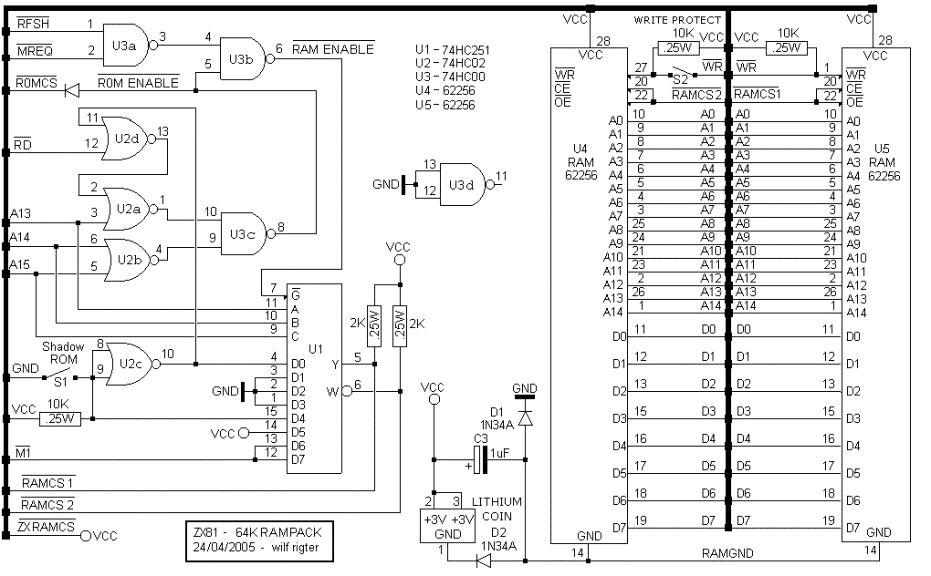
The memory from both chips is strategically allocated in 8 blocks of 8K throughout the 64K memory map.
The first RAM chip provides Basic memory between 16K and 32K normally occupied by the conventional 16K RAMPACK. This part of memory contains in order, the system variables, the Basic program, the Basic Display file, the Basic variables, various scratch pad and temporary memory locations and the machine code stack
This system memory space is tested and initialized by the ZX81 Basic OS on power up and reset and therefore the contents will normally be erased.
8K of the RAM1 chip is also located between 8K and 16K is reserved for use with popular machine code programs such ZXAS that run from that space, or with high resolution graphics programs such as WRX16 which use that space for the 256x192 bitmapped display file. This space is not initialized on reset so a hires screen or ML program are usually left intact.
The final 8K of RAM1 can be configure to reside 32K-40K used for expanded BASIC RAM space for example with the ability to DIM large arrays. This 32K-40K area is shared with RAM2 as is explained next.
The second RAM chip occupies all of the available memory space above 32K RAM in a contiguous block of write protected nonvolatile RAMDISK where programs can be saved to and loaded from.
So what about this shared block of memory? It depends on the position of S1 which configures both the 0-8K ROM and the 32-40K areas.
When S1 is open as shown, the 8K block from RAM1 is turned off and the 8K block of RAM2 occupies the 32-40K area.
This 8K block can be used for program storage or can be programmed with a modified copy of the ZX81 ROM. When S1 is closed, this nonvolatile write protected 8K block of RAM2 that was programmed in 32-40K, is overlaid on the ROM area between 0-8K. At the same time the 8K block of RAM1 is placed in the 32-40K area and becomes available as area BASIC expansion RAM.
Any ML code can be installed to run from the 0K to 8K area but the video character pattern tables cannot be changed to give new characters for the ZX display. This is because the old ZX ROM contents continue to be used for normal and pseudo hires patterns. The up side is that the 512 byte memory space between address 7680 and 8191 can now be used for new operating system code without disturbing the video display.
HOW THE 64K DECODER
WORKS
The 251 decoder provides two programmable RAMCS signals which are connected to the two 32K RAM chip Cs and OE pins. The 74HC251 memory decoder chip uses A13-A15 and the RAM ENABLE signal to select 1 or 8 inputs. If the selected input pin (0-7) is low, then the output Y at pin 5 is low and RAM1 is enabled. If the selected input pin is high then output W goes low and RAM2 is enabled.
There are some hardwired connections to these inputs. For instance, the GND connection to pin 1-3 always enables the RAM1 chip when addressed in the 8-32K range. The Vcc connected to pin 14 always enables RAM2 chip when 40–48K space is selected. When the M1 signal connected to pins 12 and 13 is low this enables the RAM1 chip so that the normal ZX video display can be executed above RAMTOP. For any other READ and WRITE memory access to this 48 to 64K address space, the RAM2 is enabled.
Next we come to pin 15 and pin 4 controlled by S1 and inverter U2a. When S1 is open as shown, connecting pin 15 to Vcc, then RAM2 is enabled in the 32-40K area and pin 4 which is GND from inverter U2c cause the 8K block in RAM1 to be turned off.
When S1 is closed then pin 15 is low and pin 4 is at Vcc. Now RAM2 is enabled in the 0-8K space overlaying the ROM while RAM1 is enabled in the 32-40K area.
ROM/RAM ACCESS DECODING
All CPU access to 0-8K address space normally enables the ROM as the ULA generates a low signal on the ROM CS line. All the ROM decoder circuit must do is to selectively disable the ROMCS line when the RAM chips are enabled. Conversely, when the ROMCS is not disabled the ROM decoder must inhibit the RAM decoding.
The ROM decoder circuit consists of U2a,b,d and U3c. The first two decode the A13-A15 lines and when these are all low and either RD is high or the SHADOW ROM switch is closed, then the ROM ENABLE line goes low and the RAM ENABLE line is high, inhibiting RAM decoding. At any other time the RAM is enabled and ROM is disabled. The RAM ENABLE signal uses both RFSH and MREQ because the RFRSH signal is asserted before MREQ, which is important for fetching hires patters from RAM.
When the S1 is closed, a high on U2c pin 10is connected to U2d pin 11. This causes pin 13 to go low and ROM ENABLE will go low whenever A13-15 are low. If RFSH or MREQ is low, the ROMCS line low signal is generated by the ULA and the ROM is accessed between 0-8K.
When the Shadow ROM switch S1 is open, U2d will be controlled by RD on pin 12 as follows:
1) If RD is high (and WR or RFSH are low) and A13-15 are low then RAM ENABLE is inhibited and ROMCS is not disabled for access between 0-8K.
2) If RD is low, then ROM access is disabled and RAM ENABLE permits RAM2 to respond to access between 0-8K.
When S1 is switched down, RAM2 in 32K–40K area is no longer accessible in that location and instead the 8K block from RAM1 is accessed. The 8K block of RAM2 becomes shadow ROM, switched to the 0-8K area from where the system boots at power up or reset. The Shadow ROM can be modified with an auto running a Basic program from system memory from power up.
You may wonder why RD is used to decode the ROM. Only when RD is low can the Shadow ROM (in RAM2) access data and machine code in the 0-8K space. When RD is high, any memory access with WR low!! or RFRSH low (for video pattern lookup) will access the old ROM contents instead.
Well that wraps it up for another project. Until next time,
enjoy
wilf