HIGH
SPEED INTERFACE 2
Revised August 13, 2005 - wilf rigter
INTRODUCTION
The
HS-2 system described here is a high speed interface between
two
TS1000 units, one of which is dedicated to executing a user
program
in the FAST mode while the other generates a continuous
video
display of the user program DFILE.
The
HS-2 system is based on the concept of HS-1.
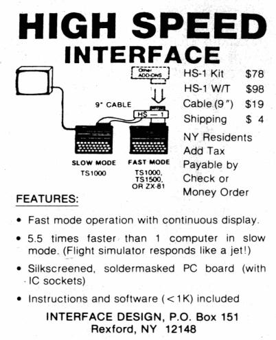
Little
is known about the HS-1 system except for some advertisements of
which
this one was taken from a March 84 SYNC magazine. I am curious to
find
out if anyone had any hands on experience with the HS-1 system.
It is
clear that two stock TS1000s were used, connected together through
an
interface card and 9” cable. According to the description, one TS1000
runs in
the FAST mode to execute the user program at near maximum speed
while
the other unexpanded TS1000 runs in the SLOW mode to display the
DFILE
of the user program that is running on the FAST TS1000. It uses
FLIGHT
SIMULATOR as an example program, which suggests that it is
compatible
with stock TS1000 programs. There are no other details that I
am
aware of but this information is enough to design a similar though
perhaps
somewhat slower system.
TS1000 FAST and SLOW mode
A TS1000
in the FAST mode can run user programs full speed while the
video
circuit is turned off so no video is displayed until the user
program
pauses.
A
TS1000 in the SLOW mode can generate a continuous video display but user
programs
run at 1/6 (60Hz) of the FAST mode speed because the Z80 CPU spends
most of
its time on generating the video display.
HIGH SPEED INTERFACE II
After
evaluating several different design approaches for transferring
data
between two TS1000 units, I settled on a Master-Slave architecture.
The
Slave memory is transferred to Master memory through an I/O interface
This is
not quite as fast as a true memory to memory interface but much
simpler
to design.
The
Master TS1000 provides a SLOW mode video display of the application
program
running in the FASYT mode on the Slave TS1000.
The
HS-2 interface provides the Master TS1000 with Direct Memory Access
to the
Slave DFILE using three I/O ports and a control program.
The
Master takes control of the Slave by using BUSRQ, which gives
access
to the entire 64K of Slave memory space.
The
Slave memory contents are addressed with a 16 bit address set up in
two 8
bit output ports and data is transferred directly from the Slave
memory,
through an input ports to the Master memory (eg DFILE to DFILE).
Slave
memory data is transferred to Master memory using arbitrary
source
and destination addresses.
For
example, after asserting BUSRQ and the BUSAK handshake, the Slave
memory
System Variables DFILE and VARS are read. Next the Slave DFILE
addresses
and length are calculated. The most significant eight
address
bits of the Slave DFILE are loaded into the MSB address latch.
The
least significant address bits are set up in B register.
The
starting address of the Master DFILE is loaded into HL and the
Slave
DFILE of up to 793 bytes is transferred in 4 blocks using the
INDR
instruction which automatically decrements the B register and the
HL
register pair. Note that using INDR, the B register is decremented
so
DFILE must be transferred in reverse order! More on this later.
HS-2 HARDWARE
The
HS-2 design approach is based on simplicity and transparency by using
five
simple TTL chips.
A
74HC32 and 74HC02 are used for I/0 port address decoding and for a
Master
Machine State decoder.
The Machine
State Decoder is basically the same circuit used in my
Turbo
clock-doubler and is required to decode whether the MASTER CPU is
running
the video routines or the control program.
A
74LS573 octal latch is used to store the MSB Slave memory address.
A
74HC541 (or an inverting 74HC540) is used as the LSB address buffer.
The
data I/O port uses a 74HC245 bi-directional buffer hardwired for input.
The
control hardware and software runs on the Master TS1000. The Master
Runs in
the SLOW mode and spends most CPU time executing video routines.
When
the CPU is free to run the control program, the machine state decoder
asserts
the BUSRQ signal on the Slave TS1000 bus. The Slave CPU responds
with
BUSACK, which enables the IC3-IC4, registers to place a specific Slave
memory
address on the Slave bus. The Master then reads the data byte at
that
Slave memory address through U5, the input port and transfers the
byte to
the Master memory. Each Slave DFILE byte is consecutively address
and transferred
from the Slave DFILE to the Master DFILE.
The
time to transfer a byte using INDR is about 6.5 us, so a complete
DFILE
can take up to 793 x 6.5us = 6ms of CPU time. Since the transfer
will be
interrupted during the SLOW video display time, the total time to
transfer
DFILE is 1.5 to 3 frames depending on the vertical frame rate.
This
time is not wasted as the Master Machine State decoder automatically
drops
the BUSRQ line during the video display, which allows the SLAVE user
program
to resume execution.
In
fact, the Slave user program only runs when the Master TS1000 is
generating
the video display which means that the Slave user program uses
more
than 80% of available Slave CPU time at 60 Hz vertical frame rate.
This
means that the FAST TS1000 user program runs 5 times faster than the
normal
60HZ SLOW mode.
The
INDR instruction decrements B register which would require that both
The
source and destination addresses decrement and DFILE be transferred in
Reverse
order. This can be problematic if DFILE is not properly formatted
(eg
after SCROLL) Two solutions are available to deal with this problem.
1) Use
a 74HC540 inverting buffer for IC3 which effectively increments LSB
address
as B register decrements. That allows the INIR instruction to be
used to
transfer DFILE from start in the normal order.
2) Use a 74HC541 for IC3. Since the Master TS1000 has 2K of RAM, there is
enough memory for two complete DFILEs. That way one Master DFILE is
updated in reverse order while the other is displayed and the Master
DFILE variable can be toggled between the two alternate DFILEs for a
properly formatted and ghost free display.
I am sure there will be some discussion, suggestions and comments before
actually building the prototype but this HS-2 circuit looks like a winner.
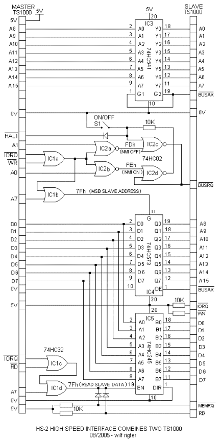
CIRCUIT DETAILS
The HS-2 circuit is sandwiched between the Master and Slave TS1000. The
HS-2 circuit is assembled on a PCB, which unlike the HS-1, is mounted on
and powered from the MASTER TS1000. This is done so that the input side
of the circuit is properly terminated. In fact, the Master TS1000 can be
powered up with the HS-2 installed but with no SLAVE TS1000 connected.
The control program checks to see if the first DFILE byte is valid N/L
character (76h) before transferring DFILE. Similarly, the SLAVE CDFLAG
system variable is checked for FAST mode so that the MASTER control
program aborts if it cannot find a FAST SLAVE or proper DFILE.
The SLAVE TS1000 is connected to the interface with a 32 conductor flat
cable. The 0V or Gnd bus is common to both TS1000 and the interface
circuit. The HS-2 interface is powered by the Master regulated +5V bus.
Not shown is the common switched 9V supply that supplies power to both
TS1000 units.
IC1 is a quad OR gate used to decode I/O RD and I/O WR signals.
IC1c/d decode /IORQ and /RD with /A7 to enable IC5 the data input Port at
Address 7Fh.
In addition, this input post enable signal also pulls the SLAVE tri-stated
MREQ and RD signals active low so that the SLAVE memory address and control
signals are decoded by the SLAVE memory addressing circuit including the ULA
(RAMCS/ROMCS) or any expansion RAMPACK. The 10K pull up resistors on MREQ,
IORQ, RD and WR avoid spurious decoding of those signals when tri-stated.
IC1a/b decode /IORQ and /WR with /A7 to enable IC4 and load the MSB of the
SLAVE memory address into the octal latch.
IC1a together with IC2a/b and A0 or A1 form a RS flip-flop which decodes
whether VIDEO is displayed or the USER program is executing.
This Machine State Latch is RESET with OUT FE when the NMI generator is
turned off (VIDEO) and SET with OUT FD when NMI is turned ON (USER).
The MS Latch is also RESET when HALT is low during the VIDEO display
and switch S1 manually RESET the MS Latch when closed.
During each vertical frame, when the MASTER TS1000 executes the USER program
during so called BLANK lines, the MS Latch is automatically SET and the
SLAVE BUSRQ line is pulled low. The SLAVE CPU responds with BUSACK which
enables the SLAVE address output ports IC3 and IC4. The SLAVE memory data is
then ready to be read through IC5 by the MASTER TS1000 control program.
The normal sequence of activating the HS-2 interface is as follows:
1) With power disconnected plug the HS-2 unit into the MASTER TS1000
2) Connect the flat cable between the HS-2 unit and the SLAVE TS1000
3) Close S1.
4) Turn on 9V power.
5) Load the control program on MASTER TS1000 (HS-2 EPROM to be added)
6) Load application program on SLAVE.
7) Run SLAVE program in FAST mode.
8) Open S1 to start the HS-2 Interface and display the MASTER TS1000 video.
9) Run MASTER control program to display the SLAVE TS1000 video.
Note that the SLAVE TS1000 must always be in FAST mode when the HS-2
Interface is active or the active BUSRQ can freeze the SLAVE TS1000.
One way to guarantee that the SLAVE is always in the FAST mode is to disable
NMI by bending pin 15 of the SLAVE ULA out of the IC socket and using a 1K
pull up resistor to the Z80 NMI line which can be added on the HS-2
interface board.
The ZX81 ROM is backward compatible with the ZX80 and on power up or RESET
tests for the presence of pulses on the NMI line to either run in the SLOW
ZX81 video mode or in the FAST ZX80 video mode.
CONTROL PROGRAM
I only have a bare outline for the control program as described above but
it should be straight forward. More error checking can be added but the
key is to make the transfer program as fast as possible.
The data port can be made bi-directional for read/write access to SLAVE
memory.
Other software can use this hardware for new applications like adding input
devices such as a keyboard or mouse or other output devices such as a LCD.
COMMENTS
More to come.
REVISION NOTES
Aug 13,2005 – spelling corrections and notes on simulating a SLAVE ZX80.